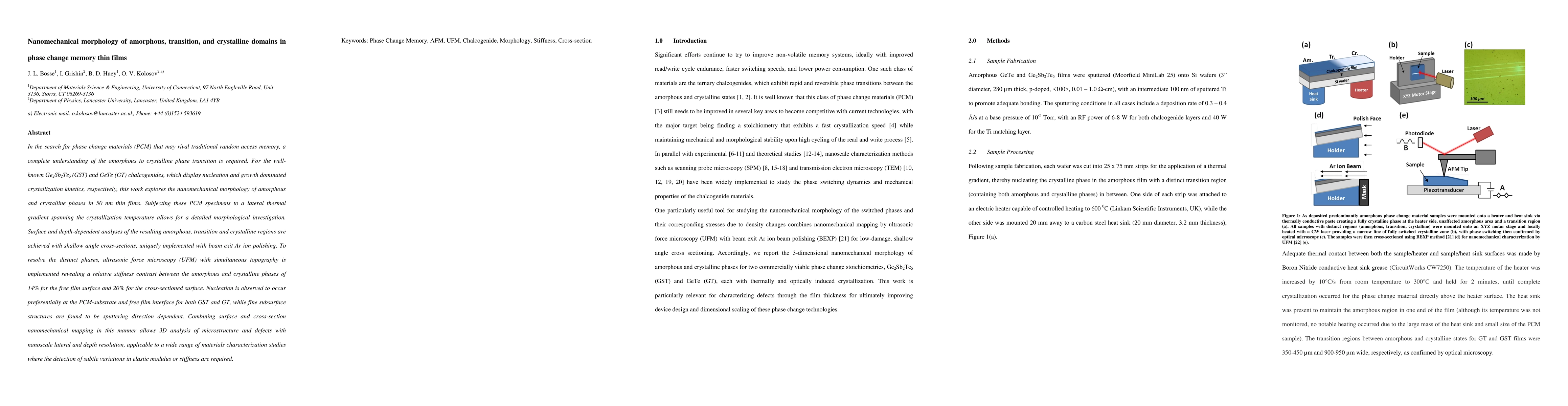
Quick Summary:

This study investigates the nanomechanical morphology of amorphous, transition, and crystalline domains in phase change memory thin films using ultrasonic force microscopy. It reveals a 14%-20% stiffness contrast between amorphous and crystalline phases, with nucleation occurring preferentially at interfaces, and provides a 3D analysis method applicable to material characterization.

Summary

In the search for phase change materials (PCM) that may rival traditional random access memory, a complete understanding of the amorphous to crystalline phase transition is required. For the well-known Ge2Sb2Te5 (GST) and GeTe (GT) chalcogenides, which display nucleation and growth dominated crystallization kinetics, respectively, this work explores the nanomechanical morphology of amorphous and crystalline phases in 50 nm thin films. Subjecting these PCM specimens to a lateral thermal gradient spanning the crystallization temperature allows for a detailed morphological investigation. Surface and depth-dependent analyses of the resulting amorphous, transition and crystalline regions are achieved with shallow angle cross-sections, uniquely implemented with beam exit Ar ion polishing. To resolve the distinct phases, ultrasonic force microscopy (UFM) with simultaneous topography is implemented revealing a relative stiffness contrast between the amorphous and crystalline phases of 14% for the free film surface and 20% for the cross-sectioned surface. Nucleation is observed to occur preferentially at the PCM-substrate and free film interface for both GST and GT, while fine subsurface structures are found to be sputtering direction dependent. Combining surface and cross-section nanomechanical mapping in this manner allows 3D analysis of microstructure and defects with nanoscale lateral and depth resolution, applicable to a wide range of materials characterization studies where the detection of subtle variations in elastic modulus or stiffness are required.

AI Key Findings

Get AI-generated insights about this paper's methodology, results, and significance.

Paper Details

PDF Preview

Download PDF

Key Terms

amorphous (0.277)
crystalline (0.264)
crystalline (0.257)
nucleation (0.199)
nucleation (0.198)
lateral (0.196)
stiffness (0.194)
film (0.180)
phases (0.179)
phases (0.173)
film (0.172)
surface (0.161)
surface (0.159)
cross (0.155)
cross (0.153)
implemented (0.148)
depth (0.147)
implemented (0.145)
depth (0.143)
materials (0.138)
Title Authors Year Actions
Tuning thermoelectric properties of Sb$_2$Te$_3$-AgSbTe$_2$ nanocomposite thin film -- synergy of band engineering and heat transport modulation
A. Ghosh, K. Agarwal, S. Munoz, Prashant Bisht, C. K. Vishwakarma, Narinder Kaur, Mujeeb Ahmad, P. Vullum, Branson D.Belle, Rajendra Singh, O. Kolosov, B. Mehta
2023
View Paper
Direct Measurements of Anisotropic Thermal Transport in γ‐InSe Nanolayers via Cross‐Sectional Scanning Thermal Microscopy
S. González-Muñoz, K. Agarwal, Eli G. Castanon, Z. Kudrynskyi, Z. Kovalyuk, J. Spièce, O. Kazakova, A. Patané, O. Kolosov
2023
View Paper
Engineering Interfacial Effects in Electron and Phonon Transport of Sb2Te3/MoS2 Multilayer for Thermoelectric ZT Above 2.0
Mujeeb Ahmad, K. Agarwal, S. Munoz, A. Ghosh, Nisha Kodan, O. Kolosov, B. Mehta
2022
View Paper
Probing the microscopic mechanisms in photovoltaic degradation behaviors of CH3NH3PbI3 perovskite films via photoconductive atomic force microscopy
Wenda Yang, Qiqi Qin, Sujuan Wu, Jinwei Gao, G. Tian, Z. Hou, Z. Fan, Xubing Lu, Deyang Chen, Xingsen Gao, Jun-ming Liu
2021
View Paper
Quantifying thermal transport in buried semiconductor nanostructures via cross-sectional scanning thermal microscopy.
J. Spièce, C. Evangeli, A. Robson, A. El Sachat, Linda Haenel, M. Alonso, M. Garriga, B. Robinson, M. Oehme, J. Schulze, F. Alzina, C. S. Sotomayor Torres, O. Kolosov
2021
View Paper
Enhancing the surface morphology for improved phase change mechanism by Sm doping in Ge2Sb2Te5 thin films
Sanjay Kumar, V. Sharma
2021
View Paper
Ion-damage-free planarization or shallow angle sectioning of solar cells for mapping grain orientation and nanoscale photovoltaic properties
Yasemin Kutes, Justin L. Luria, Yu Sun, A. Moore, B. Aguirre, J. Cruz-Campa, M. Aindow, D. Zubia, B. Huey
2017
View Paper
Nanoscale multilevel switching in Ge2Sb2Te5 thin film with conductive atomic force microscopy
Fei Yang, Ling Xu, J. Chen, Jun Xu, Yao Yu, Zhongyuan Ma, Kunji Chen
2016
View Paper
Nanothermal characterization of amorphous and crystalline phases in chalcogenide thin films with scanning thermal microscopy
J. Bosse, Maria Timofeeva, P. Tovee, Benjamin J. Robinson, B. Huey, Oleg Kolosov
2014
View Paper
Three Dimensional Mapping of Thermal Properties
J. Spièce
2019
View Paper
Scanning Probe Microscopy in Materials Science
B. Huey, Justin L. Luria, D. Bonnell
2019
View Paper

Comments (0)

This website uses cookies to ensure you get the best experience. Learn more