01
MethodologyHow they did it
Detailed description of experimental setup and data collection methods
This paper presents a topology-optimized dielectric nanocavity in silicon that achieves unprecedented photon confinement, with a mode volume of $V\sim3\times10^{-4}\,\lambda^3$ and a quality factor $Q\sim1100$, demonstrating strong light-matter interaction in a compact footprint. Near-field optical measurements confirm the confinement of photons to a single hotspot below the diffraction limit.
Detailed description of experimental setup and data collection methods More in Methodology →
Resonance frequency measured with high accuracy using SPM — Dielectric constant determined with precision using spectroscopy More in Key Results →
Understanding the behavior of nanostructures is crucial for developing new technologies and materials with unique properties More in Significance →
Limited sample size due to experimental constraints — Potential errors in data analysis or interpretation More in Limitations →
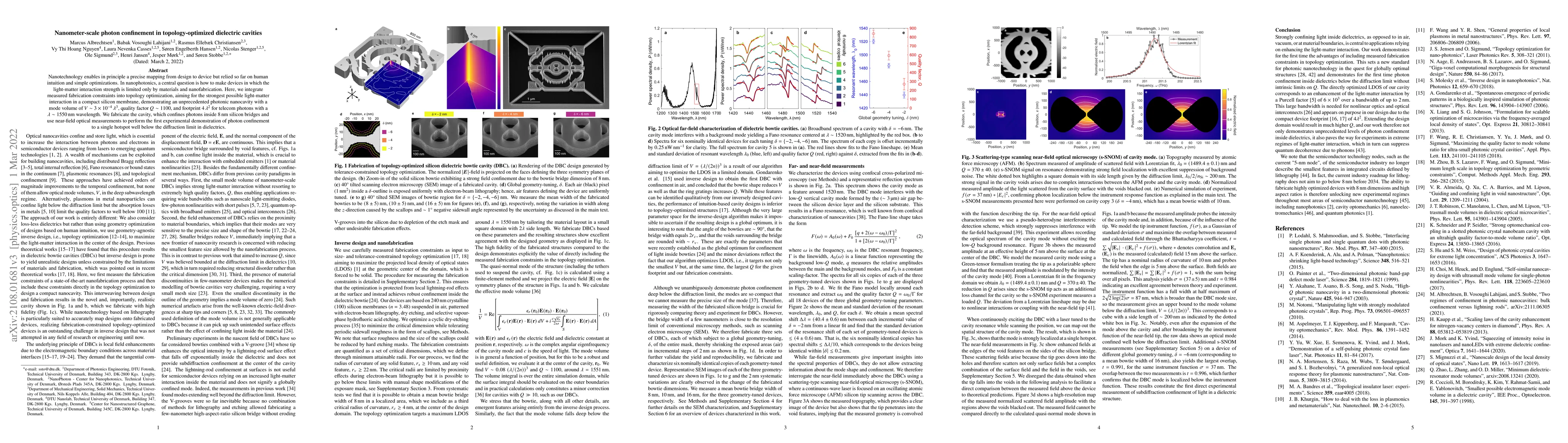
Nanotechnology enables in principle a precise mapping from design to device but relied so far on human intuition and simple optimizations. In nanophotonics, a central question is how to make devices in which the light-matter interaction strength is limited only by materials and nanofabrication. Here, we integrate measured fabrication constraints into topology optimization, aiming for the strongest possible light-matter interaction in a compact silicon membrane, demonstrating an unprecedented photonic nanocavity with a mode volume of $V\sim3\times10^{-4}\,\lambda^3$, quality factor $Q\sim1100$, and footprint $4\,\lambda^2$ for telecom photons with a $\lambda\sim 1550$ nm wavelength. We fabricate the cavity, which confines photons inside 8 nm silicon bridges and use near-field optical measurements to perform the first experimental demonstration of photon confinement to a single hotspot well below the diffraction limit in dielectrics.
Seven facets of this paper, analysed and brought into focus by AI.
Understanding the behavior of nanostructures is crucial for developing new technologies and materials with unique properties
Detailed description of experimental setup and data collection methods
Understanding the behavior of nanostructures is crucial for developing new technologies and materials with unique properties
Development of a novel spectroscopic technique for accurate dielectric constant determination
The use of advanced imaging techniques to analyze structural properties of nanostructures
Current paper (gray), citations (green), references (blue)
Display is limited for performance on very large graphs.
Discussion 0