Summary

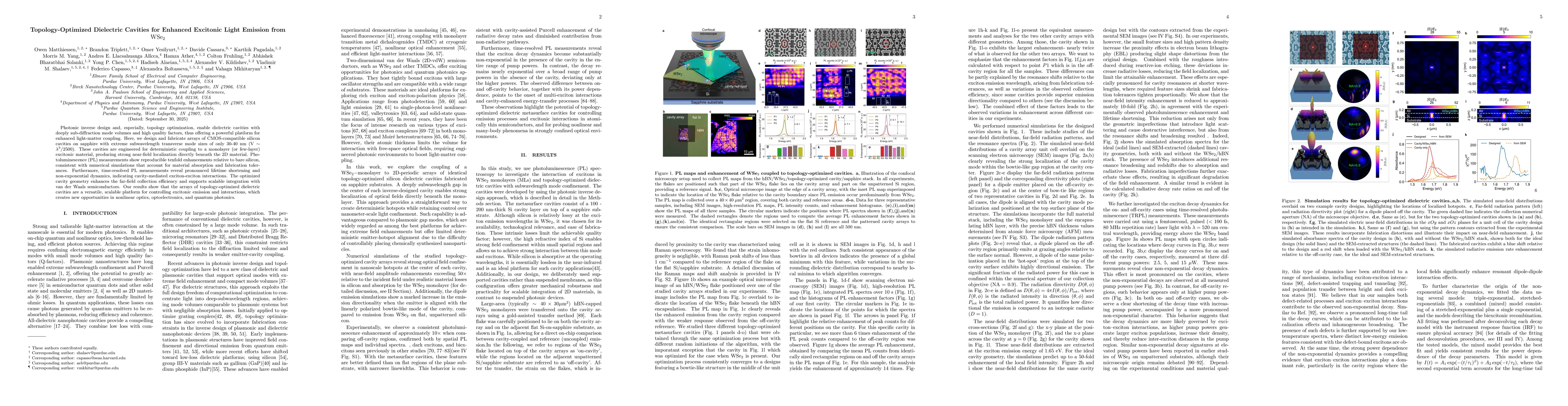
Photonic inverse design and, especially, topology optimization, enable dielectric cavities with deeply sub-diffraction mode volumes and high quality factors, thus offering a powerful platform for enhanced light-matter coupling. Here, we design and fabricate arrays of CMOS-compatible silicon cavities on sapphire with extreme subwavelength transverse mode sizes of only 30-40 nm ($\rm V\sim\lambda^3/2500$). These cavities are engineered for deterministic coupling to a monolayer (or few-layer) excitonic material, producing strong near-field localization directly beneath the 2D material. Photoluminescence (PL) measurements show reproducible tenfold enhancements relative to bare silicon, consistent with numerical simulations that account for material absorption and fabrication tolerances. Furthermore, time-resolved PL measurements reveal pronounced lifetime shortening and non-exponential dynamics, indicating cavity-mediated exciton-exciton interactions. The optimized cavity geometry enhances the far-field collection efficiency and supports scalable integration with van der Waals semiconductors. Our results show that the arrays of topology-optimized dielectric cavities are a versatile, scalable platform for controlling excitonic emission and interactions, which creates new opportunities in nonlinear optics, optoelectronics, and quantum photonics.

AI Key Findings

Generated Oct 01, 2025

Methodology

The study employed low-temperature photoluminescence (PL) spectroscopy and time-resolved measurements to analyze exciton and trion dynamics in monolayer WSe2. Spatially resolved lifetime mapping was conducted to investigate the effects of cavity coupling on emission characteristics.

Key Results

  • A significant reduction in the short decay time (τ1) was observed for on-cavity emission compared to off-cavity emission.
  • The stretching exponent (β) showed a nonlinear dependence on pump power, indicating complex recombination mechanisms.
  • The effective decay time exhibited a power-law dependence, with distinct behavior for on- and off-cavity regions.

Significance

This research provides critical insights into the interplay between cavity coupling and non-radiative recombination in 2D semiconductors, which is essential for optimizing optoelectronic devices and understanding light-matter interactions at the nanoscale.

Technical Contribution

The work introduces a mixed-model fitting approach that combines Lorentzian and Gaussian components to accurately characterize complex PL decay profiles, enabling precise extraction of lifetime parameters and energy level information.

Novelty

This study uniquely combines spatially resolved lifetime mapping with power-dependent PL spectroscopy to simultaneously analyze both temporal and energetic characteristics of excitonic states, offering a comprehensive understanding of cavity-coupled emission dynamics.

Limitations

  • The off-cavity measurements had lower signal-to-noise ratios, limiting the precision of fit uncertainties.
  • The spatial resolution of lifetime maps was constrained by mechanical drift during long acquisition periods.

Future Work

  • Investigating the role of defect states in modifying recombination dynamics under different excitation conditions.
  • Exploring the impact of varying cavity geometries on photon statistics and coherence properties.
  • Developing advanced fitting models to account for multiple recombination pathways simultaneously.

Paper Details

PDF Preview

Download PDF

Comments (0)

This website uses cookies to ensure you get the best experience. Learn more