Publication
Metrics
AI Quick Summary
This paper presents a method for fabricating large-area electron phase plates using electron-beam lithography and reactive-ion-etching, enhancing throughput and active area. The developed phase plates enable electron wavefront shaping, paving the way for novel dark-field electron microscopy and tunable electron phase plates.
Paper Preview
Abstract
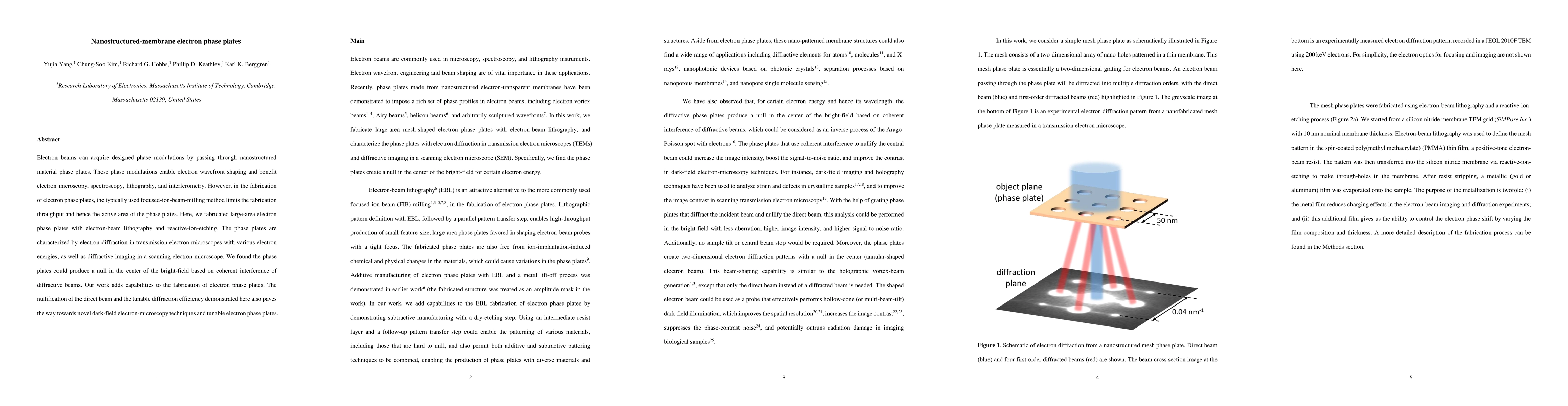
Electron beams can acquire designed phase modulations by passing through nanostructured material phase plates. These phase modulations enable electron wavefront shaping and benefit electron microscopy, spectroscopy, lithography, and interferometry. However, in the fabrication of electron phase plates, the typically used focused-ion-beam-milling method limits the fabrication throughput and hence the active area of the phase plates. Here, we fabricated large-area electron phase plates with electron-beam lithography and reactive-ion-etching. The phase plates are characterized by electron diffraction in transmission electron microscopes with various electron energies, as well as diffractive imaging in a scanning electron microscope. We found the phase plates could produce a null in the center of the bright-field based on coherent interference of diffractive beams. Our work adds capabilities to the fabrication of electron phase plates. The nullification of the direct beam and the tunable diffraction efficiency demonstrated here also paves the way towards novel dark-field electron-microscopy techniques and tunable electron phase plates.
AI Key Findings
Get AI-generated insights about this paper's methodology, results, significance, and more — seven facets brought into focus.
Impact
Paper Details
Authors
PDF Preview
Key Terms
Citation Network
Current paper (gray), citations (green), references (blue)
Display is limited for performance on very large graphs.
Discussion 0