Operando Electron Microscopy of Nanoscale Electronic Devices on Non-Conductive Substrates
Publication
Metrics
Paper Preview
Abstract
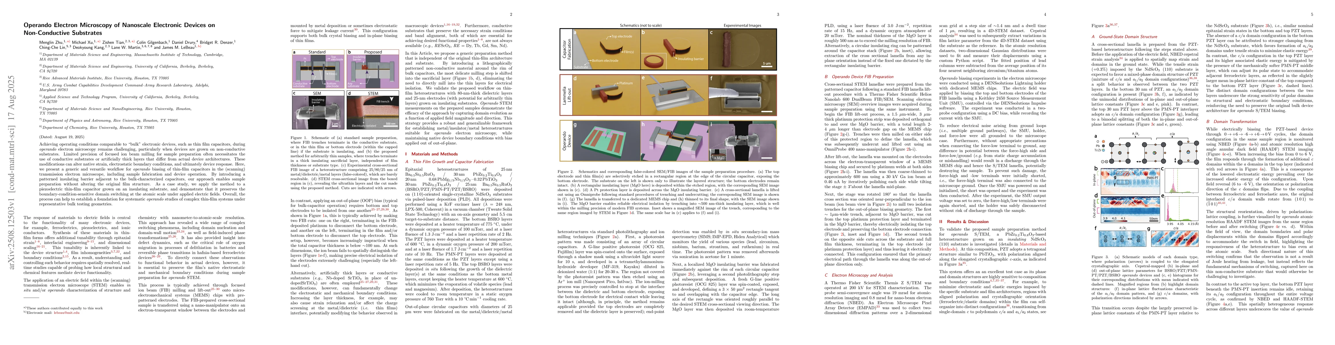
Achieving operating conditions comparable to ``bulk'' electronic devices, such as thin film capacitors, during \textit{operando} electron microscopy remains challenging, particularly when devices are grown on non-conductive substrates. Limited precision of focused ion beam milling for sample preparation often necessitates the use of conductive substrates or artificially thick layers that differ from actual device architectures. These modifications can alter native strain, electrostatic boundary conditions, and ultimately device response. Here, we present a generic and versatile workflow for \textit{operando} biasing of thin-film capacitors in the (scanning) transmission electron microscope, including sample fabrication and device operation. By introducing a patterned insulating barrier adjacent to the bulk-characterized capacitors, our approach enables sample preparation without altering the original film structure. As a case study, we apply the method to a piezoelectric thin-film capacitor grown on an insulating substrate, and demonstrate that it preserves the boundary-condition-sensitive domain switching at the atomic scale under applied electric fields. Overall, the process can help to establish a foundation for systematic \textit{operando} studies of complex thin-film systems under representative bulk testing geometries.
AI Key Findings
Get AI-generated insights about this paper's methodology, results, significance, and more — seven facets brought into focus.
Discussion 0