Publication
Metrics
AI Quick Summary
Researchers developed a method for creating precise p-type nanostructures on silicon using scanning tunneling microscopy, achieving sheet resistivities of 300 hinspace ext{ extcircled{}} extOmega}. {
Paper Preview
Abstract
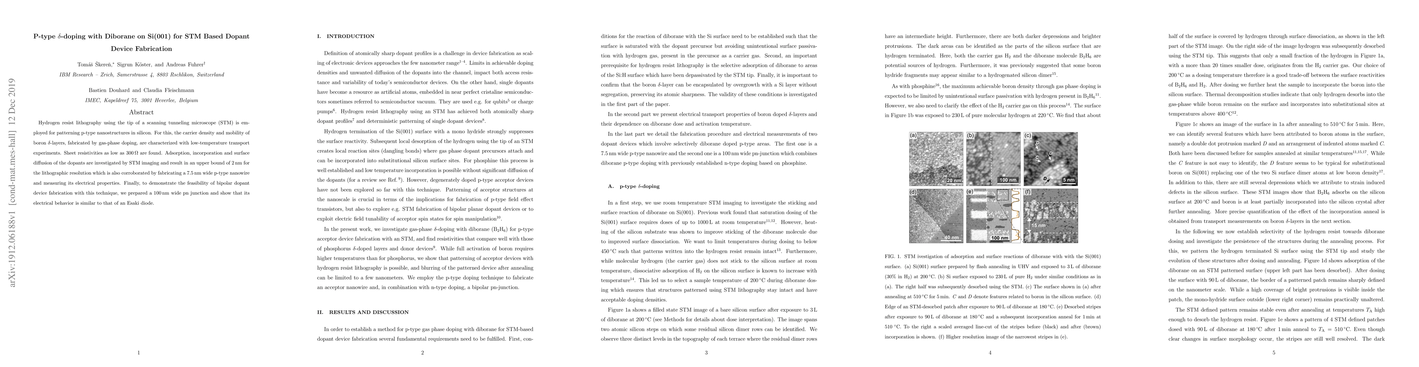
Hydrogen resist lithography using the tip of a scanning tunneling microscope (STM) is employed for patterning p-type nanostructures in silicon. For this, the carrier density and mobility of boron $\delta$-layers, fabricated by gas-phase doping, are characterized with low-temperature transport experiments. Sheet resistivities as low as $300\thinspace\Omega$ are found. Adsorption, incorporation and surface diffusion of the dopants are investigated by STM imaging and result in an upper bound of 2\,nm for the lithographic resolution which is also corroborated by fabricating a 7.5\,nm wide p-type nanowire and measuring its electrical properties. Finally, to demonstrate the feasibility of bipolar dopant device fabrication with this technique, we prepared a 100\,nm wide pn junction and show that its electrical behavior is similar to that of an Esaki diode.
AI Key Findings
Get AI-generated insights about this paper's methodology, results, significance, and more — seven facets brought into focus.
Impact
Paper Details
Authors
PDF Preview
Key Terms
Citation Network
Current paper (gray), citations (green), references (blue)
Display is limited for performance on very large graphs.
Discussion 0