Summary
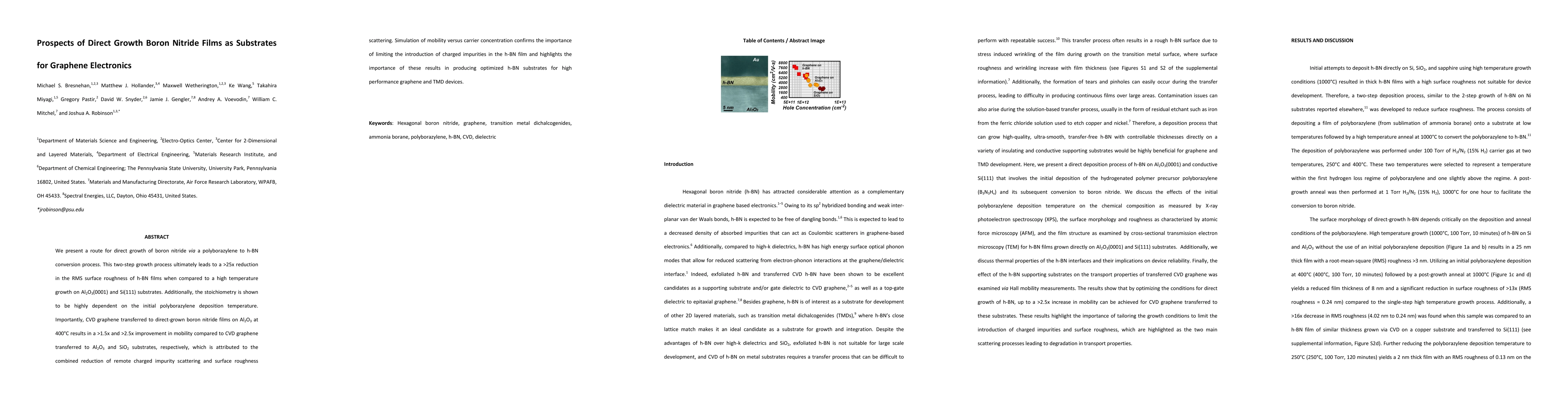
We present a route for direct growth of boron nitride via a polyborazylene to h-BN conversion process. This two-step growth process ultimately leads to a >25x reduction in the RMS surface roughness of h-BN films when compared to a high temperature growth on Al2O3(0001) and Si(111) substrates. Additionally, the stoichiometry is shown to be highly dependent on the initial polyborazylene deposition temperature. Importantly, CVD graphene transferred to direct-grown boron nitride films on Al2O3 at 400{\deg}C results in a >1.5x and >2.5x improvement in mobility compared to CVD graphene transferred to Al2O3 and SiO2 substrates, respectively, which is attributed to the combined reduction of remote charged impurity scattering and surface roughness scattering. Simulation of mobility versus carrier concentration confirms the importance of limiting the introduction of charged impurities in the h-BN film and highlights the importance of these results in producing optimized h-BN substrates for high performance graphene and TMD devices.
AI Key Findings
Get AI-generated insights about this paper's methodology, results, and significance.
Paper Details
PDF Preview
Key Terms
Citation Network
Current paper (gray), citations (green), references (blue)
Display is limited for performance on very large graphs.
Similar Papers
Found 4 papersUnidirectional domain growth of hexagonal boron nitride thin films
Xiang Zhang, Chenxi Li, Pulickel M. Ajayan et al.
| Title | Authors | Year | Actions |
|---|
Comments (0)