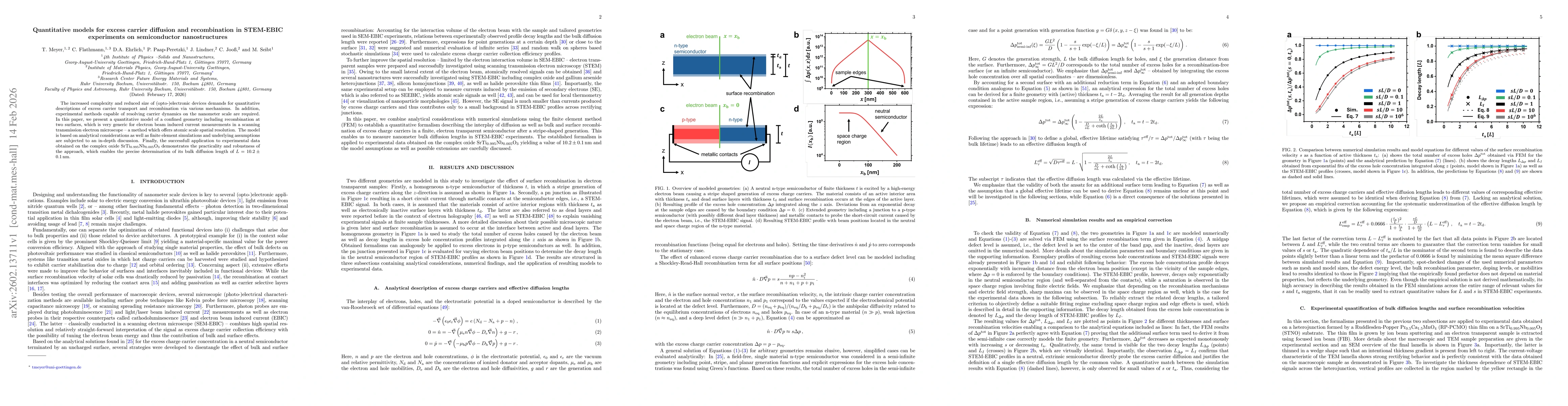
Quantitative models for excess carrier diffusion and recombination in STEM-EBIC experiments on semiconductor nanostructures
Publication
Metrics
Paper Preview
Abstract
The increased complexity and reduced size of (opto-)electronic devices demands for quantitative descriptions of excess carrier transport and recombination via various mechanisms. In addition, experimental methods capable of resolving carrier dynamics on the nanometer scale are required. In this paper, we present a quantitative model of a confined geometry including recombination at two surfaces, which is very generic for electron beam induced current measurements in a scanning transmission electron microscope - a method which offers atomic scale spatial resolution. The model is based on analytical considerations as well as finite element simulations and underlying assumptions are subjected to an in-depth discussion. Finally, the successfull application to experimental data obtained on the complex oxide SrTi0.995Nb0.005O3 demonstrates the practicality and robustness of the approach, which enables the precise determination of its bulk diffusion length of L = 10.2 +- 0.1 nm.
AI Key Findings
Get AI-generated insights about this paper's methodology, results, significance, and more — seven facets brought into focus.
Discussion 0