Academic Profile
Statistics
Similar Authors
Papers on arXiv
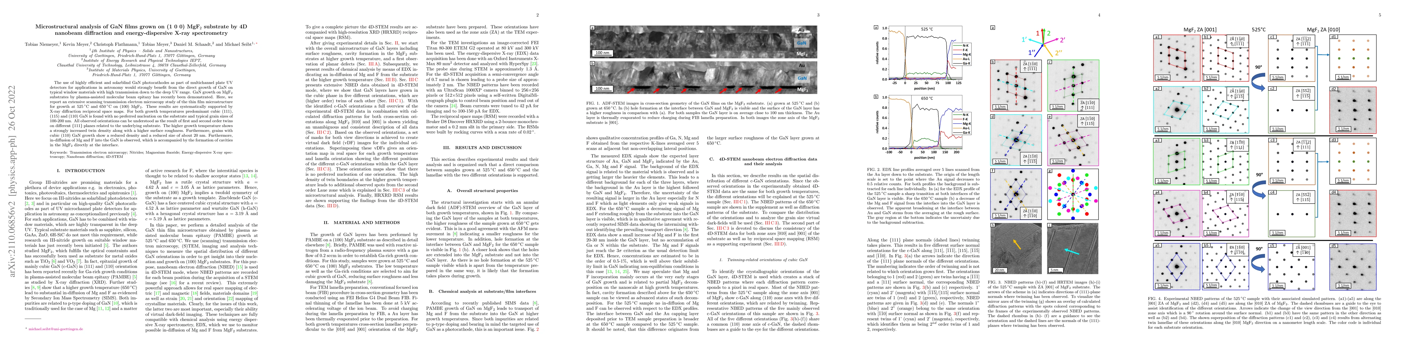
The use of highly efficient and solarblind GaN photocathodes as part of multichannel plate UV detectors for applications in astronomy would strongly benefit from the direct growth of GaN on typical ...
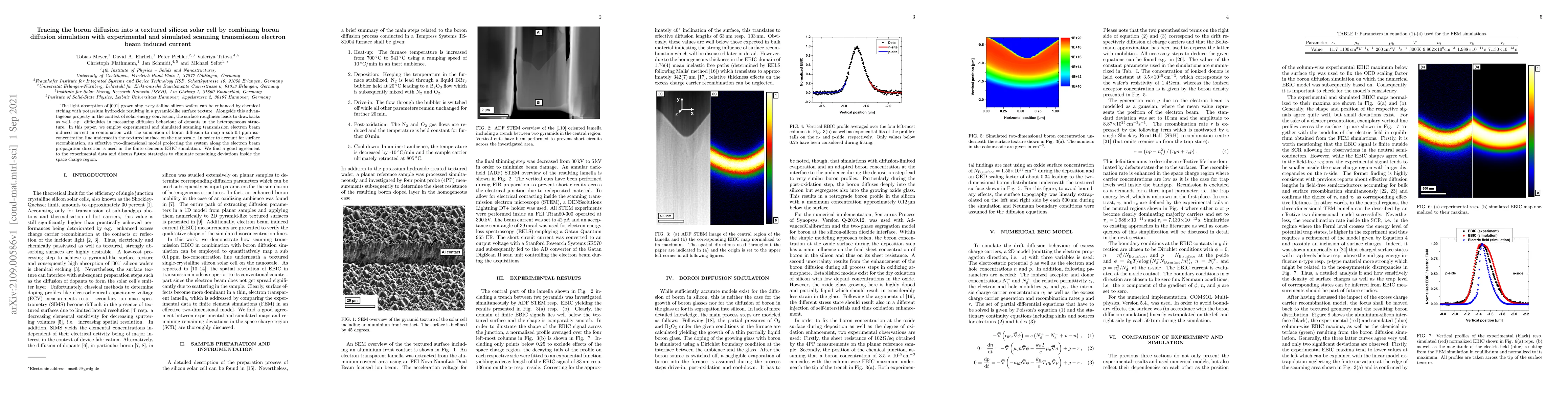
The light absorption of [001] grown single-crystalline silicon wafers can be enhanced by chemical etching with potassium hydroxide resulting in a pyramid-like surface texture. Alongside this advanta...
In this work, we introduce the platform of plasmonic Doppler grating (PDG) to experimentally investigate the enhancement effect of plasmonic gratings in the input and output beams of nonlinear surfa...
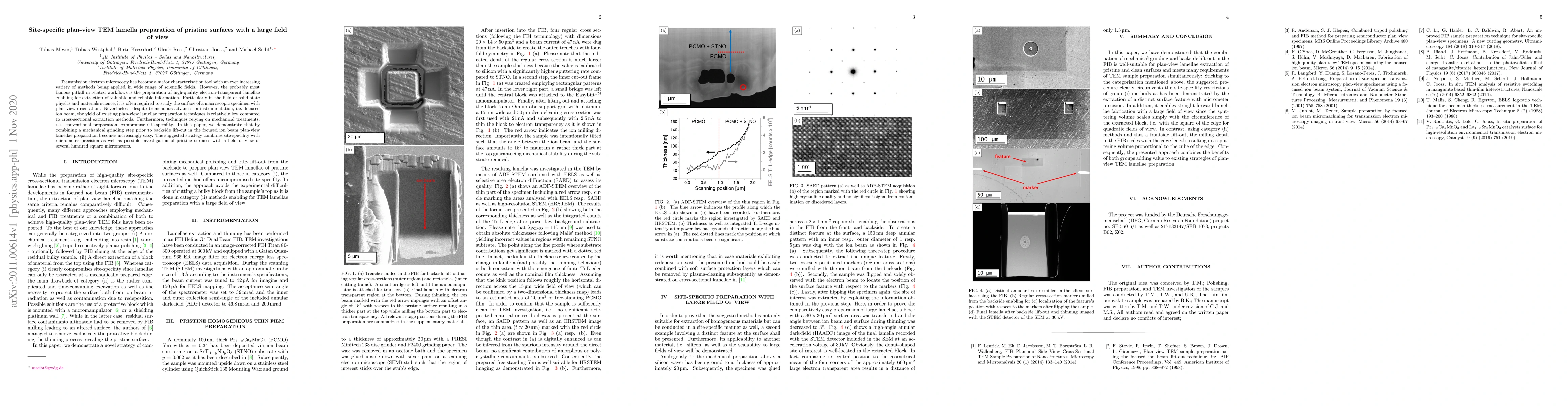
Transmission electron microscopy has become a major characterisation tool with an ever increasing variety of methods being applied in wide range of scientific fields. However, the probably most famo...
Two-Photon Microscopy (TPM) can provide three-dimensional morphological and functional contrast in vivo. Through proper staining, TPM can be utilized to create virtual, H&E equivalent images and thu...
Molecular beam epitaxy (MBE) is a state-of-the-art technique for depositing thin films with precise stoichiometric control. However, when depositing oxides of perovskite-type ABO3, this process become...

The BeEST experiment is measuring the ${}^{7}$Li recoil spectrum from the decay of ${}^{7}$Be implanted into Ta-based sensors to provide the most stringent limits on the existence of sterile neutrinos...
Grain boundaries (GBs) in oxide perovskites significantly influence their functional properties. This study examines the atomic-scale structure and composition of a faceted asymmetric grain boundary i...
Momentum-resolved scanning transmission electron microscopy (MRSTEM) is a powerful phase-contrast technique that can map lateral magnetic and electric fields ranging from the micrometer to the subatom...
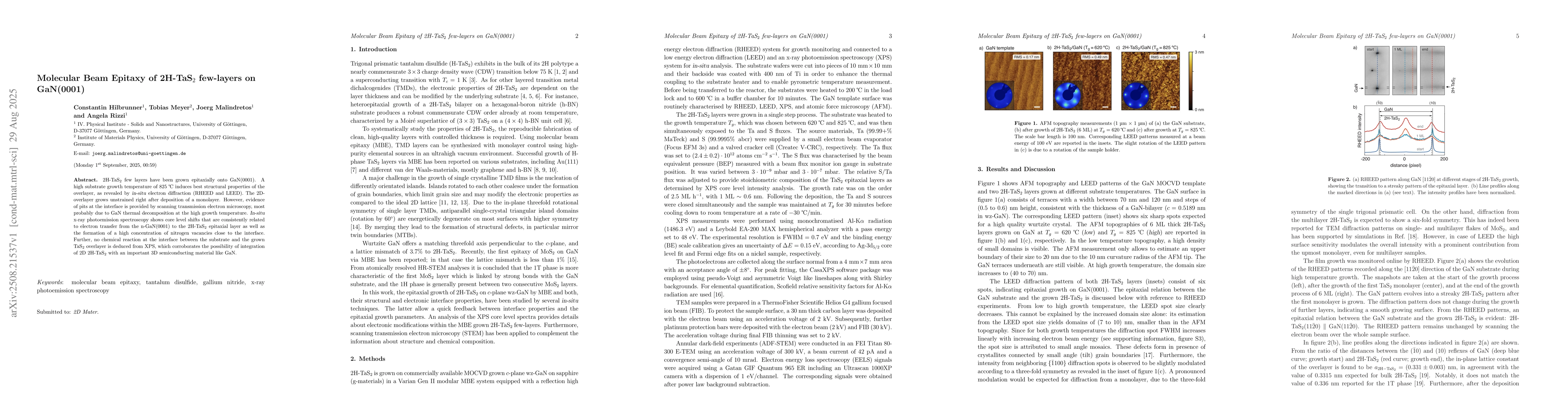
2H-TaS$_2$ few layers have been grown epitaxially onto GaN(0001). A high substrate growth temperature of 825$^{\circ}$C induces best structural properties of the overlayer, as revealed by in-situ elec...
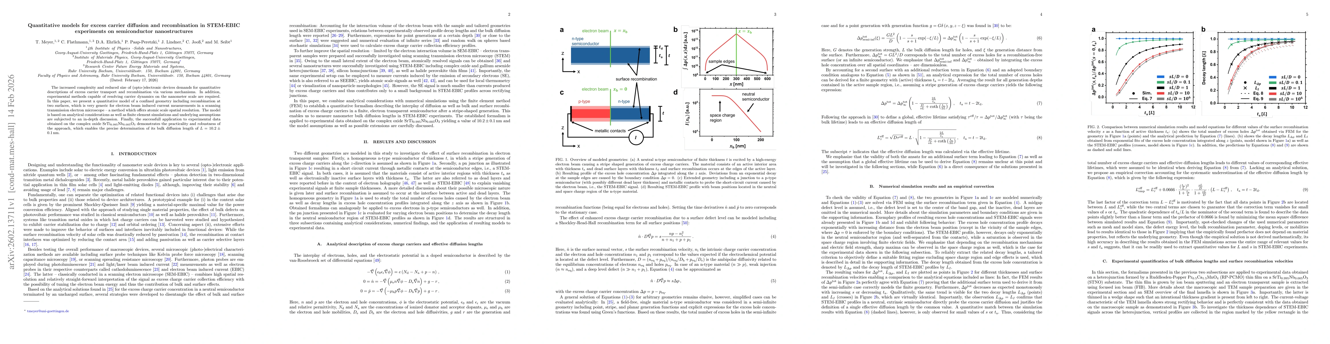
The increased complexity and reduced size of (opto-)electronic devices demands for quantitative descriptions of excess carrier transport and recombination via various mechanisms. In addition, experime...