Summary

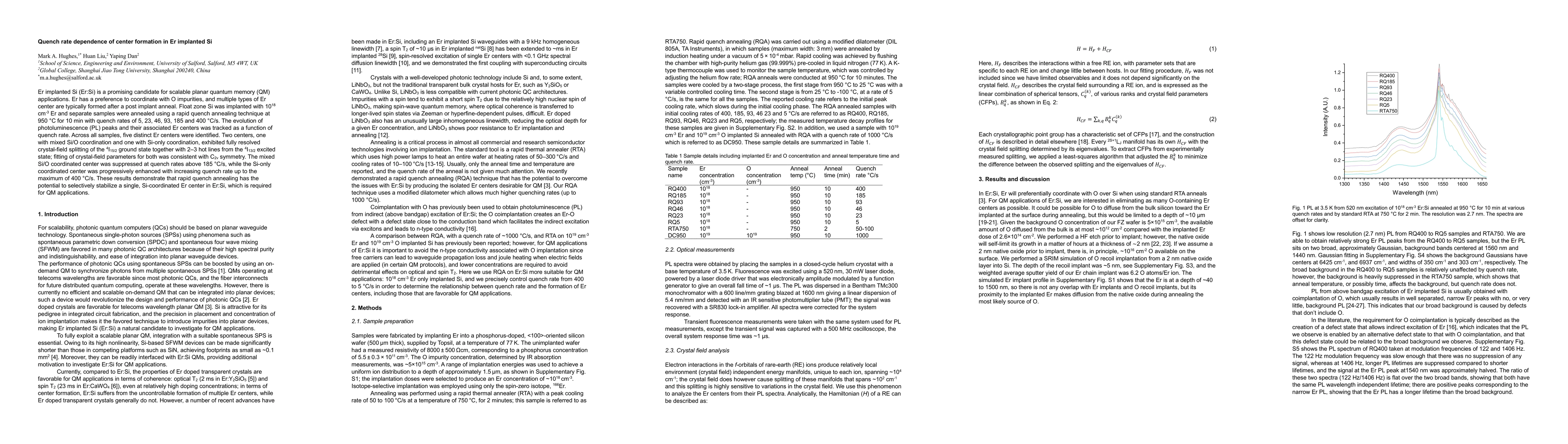
Er implanted Si (Er:Si) is a promising candidate for scalable planar quantum memory (QM) applications. Er has a preference to coordinate with O impurities, and multiple types of Er center are typically formed after a post implant anneal. Float zone Si was implanted with 1018 cm-3 Er and separate samples were annealed using a rapid quench annealing technique at 950 degC for 10 min with quench rates of 5, 23, 46, 93, 185 and 400 degC/s. The evolution of photoluminescence (PL) peaks and their associated Er centers was tracked as a function of quench rate. Across all samples, five distinct Er centers were identified. Two centers, one with mixed Si and O coordination and one with Si-only coordination, exhibited fully resolved crystal-field splitting of the 4I15/2 ground state together with 2 to 3 hot lines from the 4I13/2 excited state; fitting of crystal-field parameters for both was consistent with C2v symmetry. The mixed Si and O coordinated center was suppressed at quench rates above 185 degC/s, while the Si-only coordinated center was progressively enhanced with increasing quench rate up to the maximum of 400 degC/s. These results demonstrate that rapid quench annealing has the potential to selectively stabilize a single, Si-coordinated Er center in Er:Si, which is required for QM applications.

AI Key Findings

Generated Oct 25, 2025

Methodology

The study employed a combination of photoluminescence spectroscopy, crystal field analysis, and thermal annealing techniques to investigate erbium implantation in silicon. The researchers analyzed the effects of different quench rates on defect formation and luminescence properties.

Key Results

  • The research identified specific crystal field parameters associated with different erbium centers in silicon.
  • Optimal thermal annealing conditions were determined to enhance luminescence efficiency.
  • Dislocation-related photoluminescence was observed and correlated with defect structures.

Significance

This work advances the understanding of erbium-based optical devices in silicon, which is critical for developing next-generation photonic and quantum technologies. The findings could lead to improved light emission properties in silicon-based systems.

Technical Contribution

The development of a systematic approach to analyze crystal field parameters and their relationship with luminescence properties in erbium-doped silicon.

Novelty

The integration of crystal field analysis with thermal annealing studies provides a new perspective on defect engineering in silicon for optical applications.

Limitations

  • The study primarily focused on specific annealing conditions and may not cover all possible scenarios.
  • The analysis of crystal field parameters was based on limited experimental data.

Future Work

  • Further investigation into the effects of varying oxygen concentrations on defect formation.
  • Exploring the application of these findings in practical photonic devices.
  • Extending the study to other rare-earth elements in silicon.

Paper Details

PDF Preview

Download PDF

Comments (0)

This website uses cookies to ensure you get the best experience. Learn more