Academic Profile
Statistics
Similar Authors
Papers on arXiv
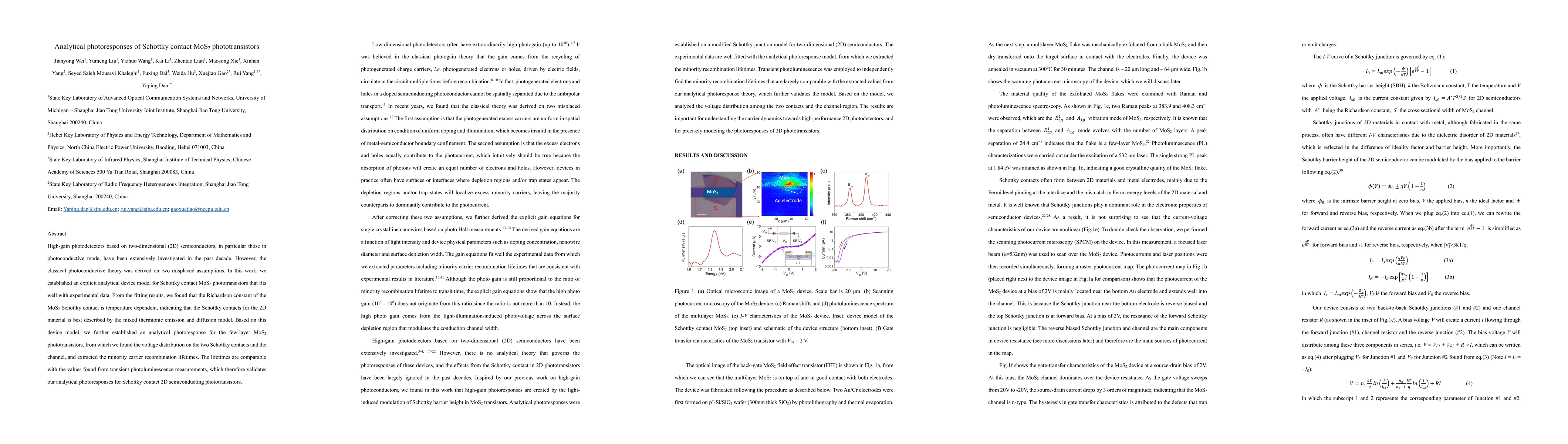
High-gain photodetectors based on two-dimensional (2D) semiconductors, in particular those in photoconductive mode, have been extensively investigated in the past decade. However, the classical phot...
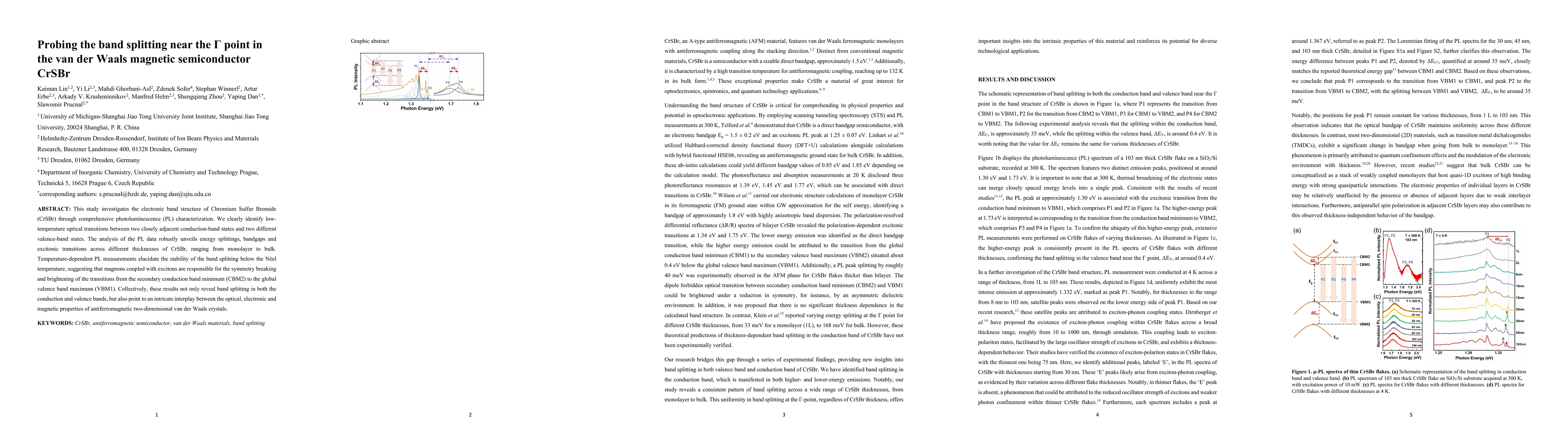
This study investigates the electronic band structure of Chromium Sulfur Bromide (CrSBr) through comprehensive photoluminescence (PL) characterization. We clearly identify low-temperature optical tr...
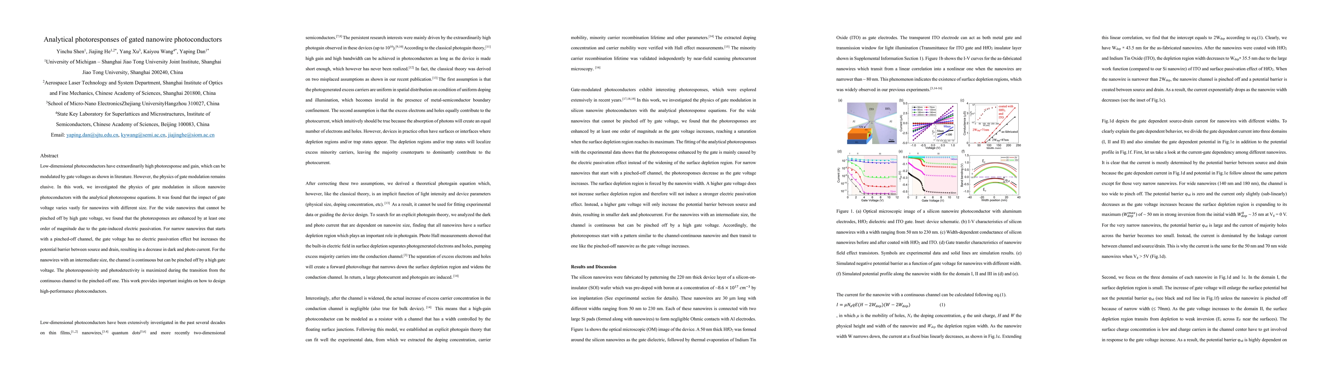
Low-dimensional photoconductors have extraordinarily high photoresponse and gain, which can be modulated by gate voltages as shown in literature. However, the physics of gate modulation remains elus...
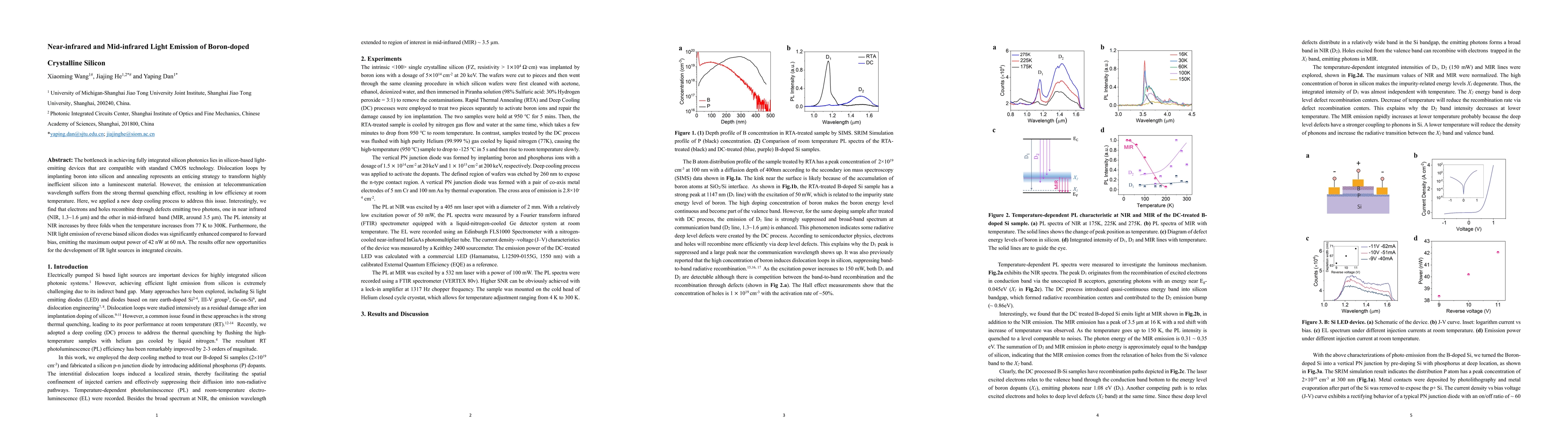
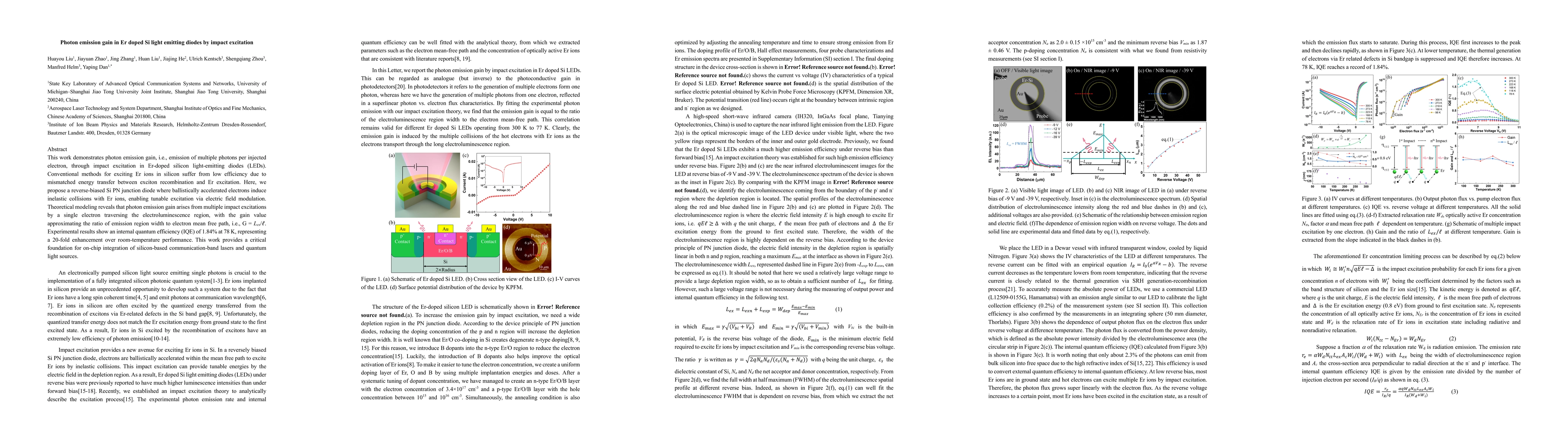
The bottleneck in achieving fully integrated silicon photonics lies in silicon-based light-emitting devices that are compatible with standard CMOS technology. Dislocation loops by implanting boron i...
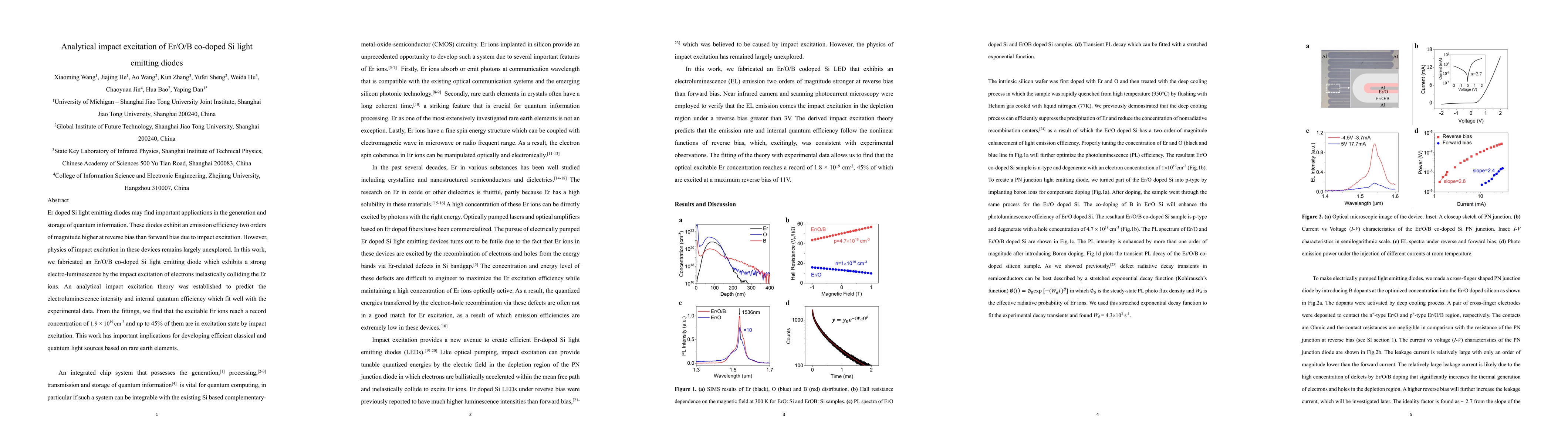
Er doped Si light emitting diodes may find important applications in the generation and storage of quantum information. These diodes exhibit an emission efficiency two orders of magnitude higher at ...
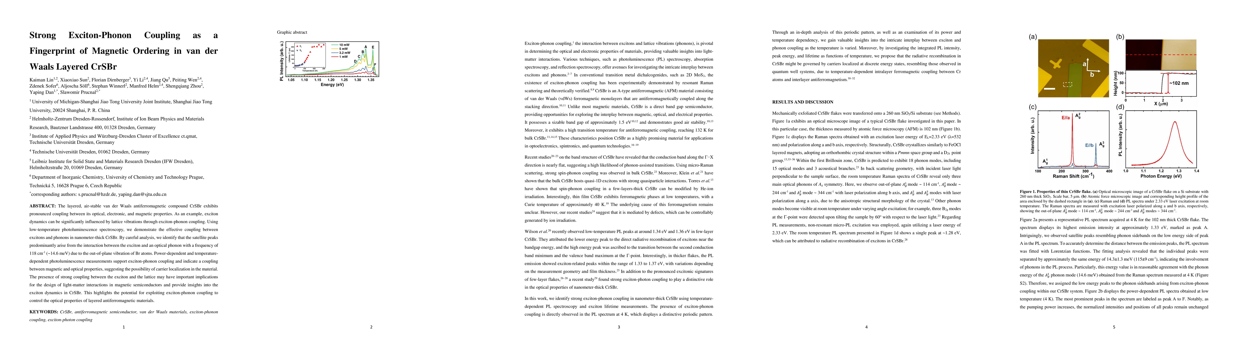
The layered, air-stable van der Waals antiferromagnetic compound CrSBr exhibits pronounced coupling between its optical, electronic, and magnetic properties. As an example, exciton dynamics can be s...
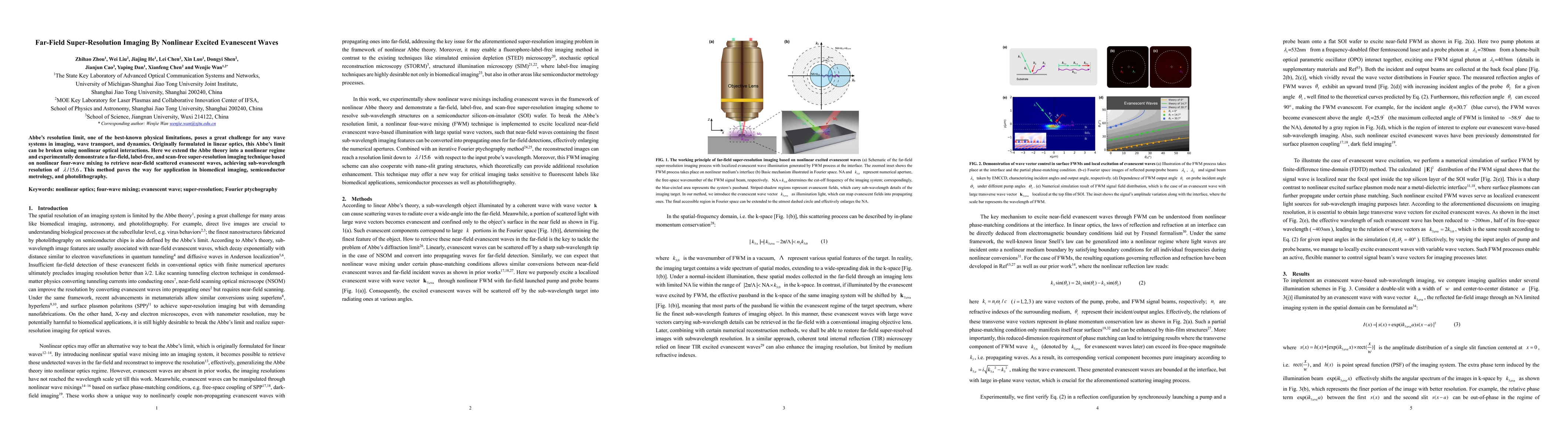
Abbe's resolution limit, one of the best-known physical limitations, poses a great challenge for any wave systems in imaging, wave transport, and dynamics. Originally formulated in linear optics, th...
Silicon-based light sources including light-emitting diodes (LEDs) and laser diodes (LDs) for information transmission are urgently needed for developing monolithic integrated silicon photonics. Sil...
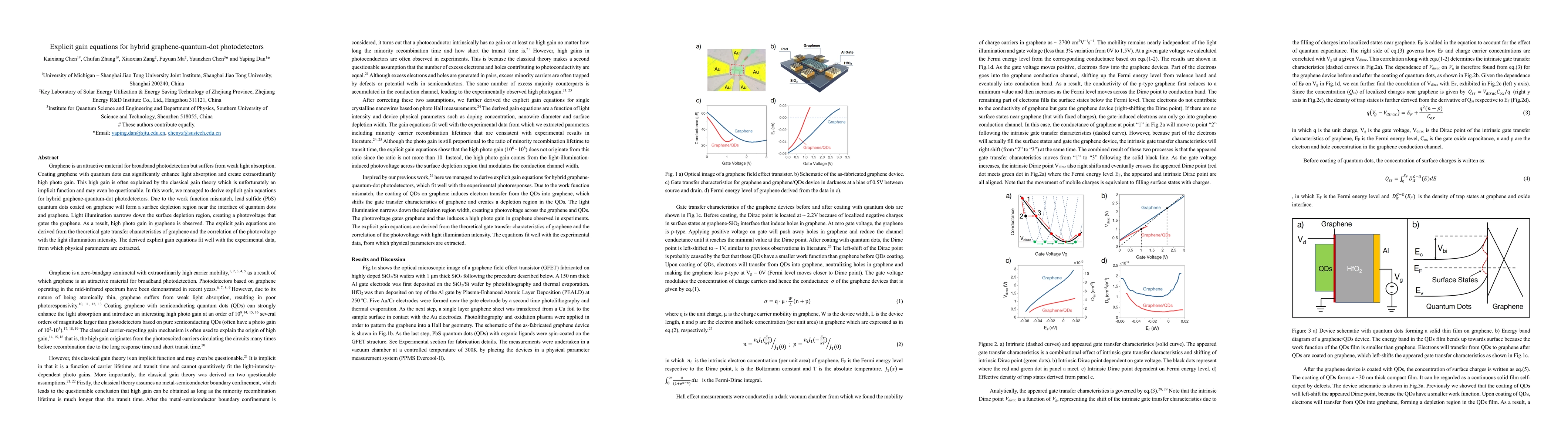
Graphene is an attractive material for broadband photodetection but suffers from weak light absorption. Coating graphene with quantum dots can significantly enhance light absorption and create extra...
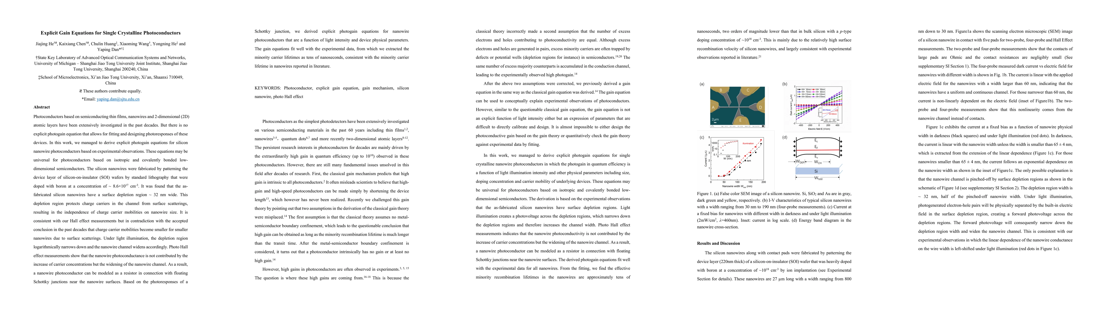
Photoconductors based on semiconducting thin films, nanowires and 2-dimensional atomic layers have been extensively investigated. But there is no explicit photogain equation that allows for fitting ...
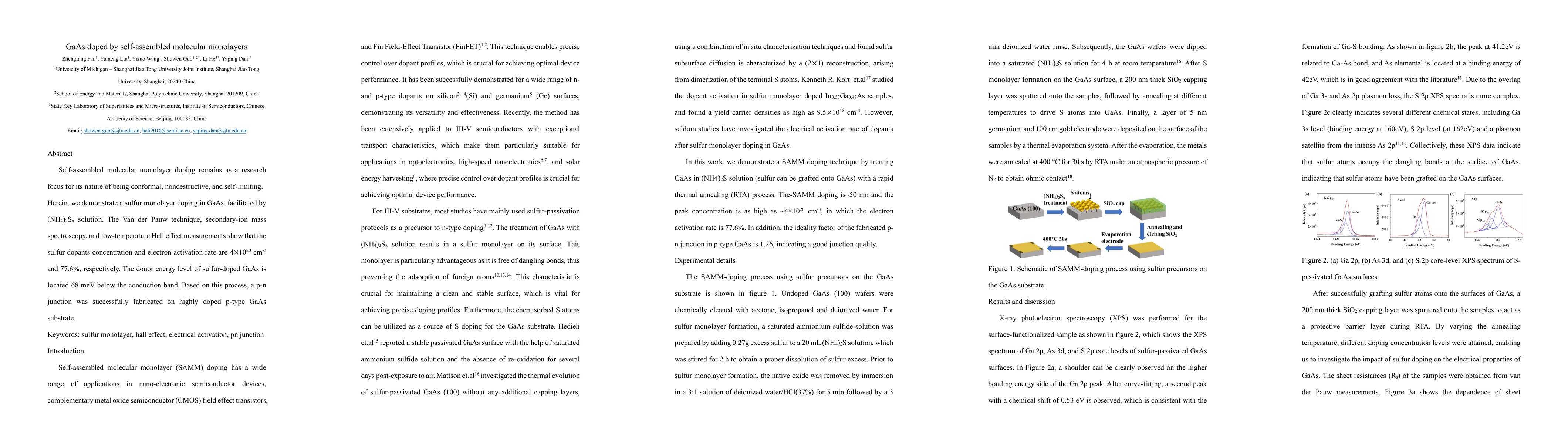
Self-assembled molecular monolayer doping remains as a research focus for its nature of being conformal, nondestructive, and self-limiting. Herein, we demonstrate a sulfur monolayer doping in GaAs, fa...
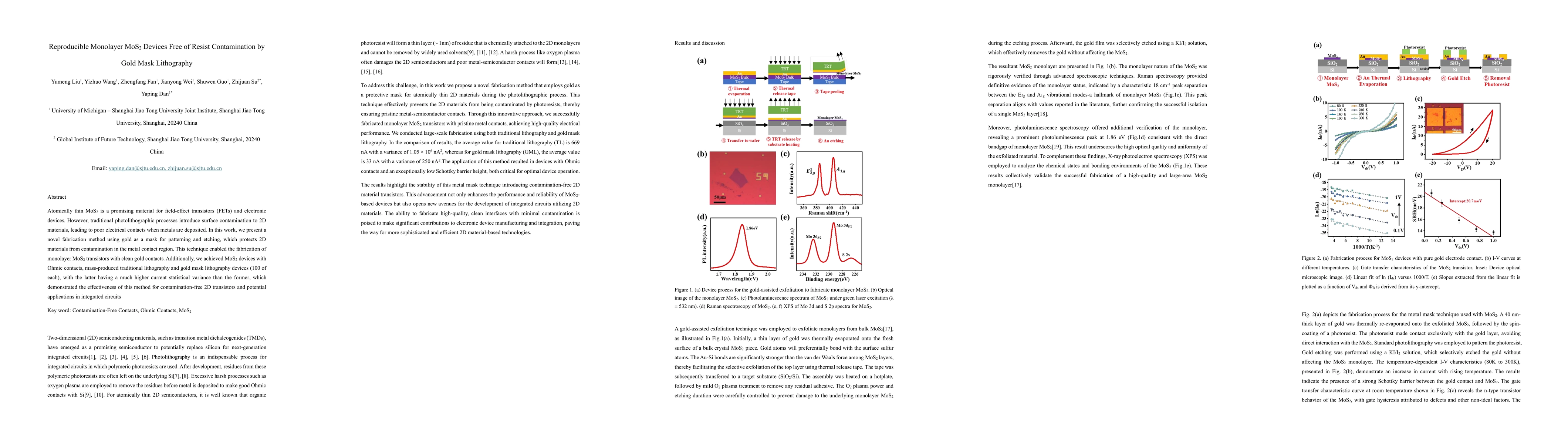
Atomically thin MoS2 is a promising material for field-effect transistors (FETs) and electronic devices. However, traditional photolithographic processes introduce surface contamination to 2D material...
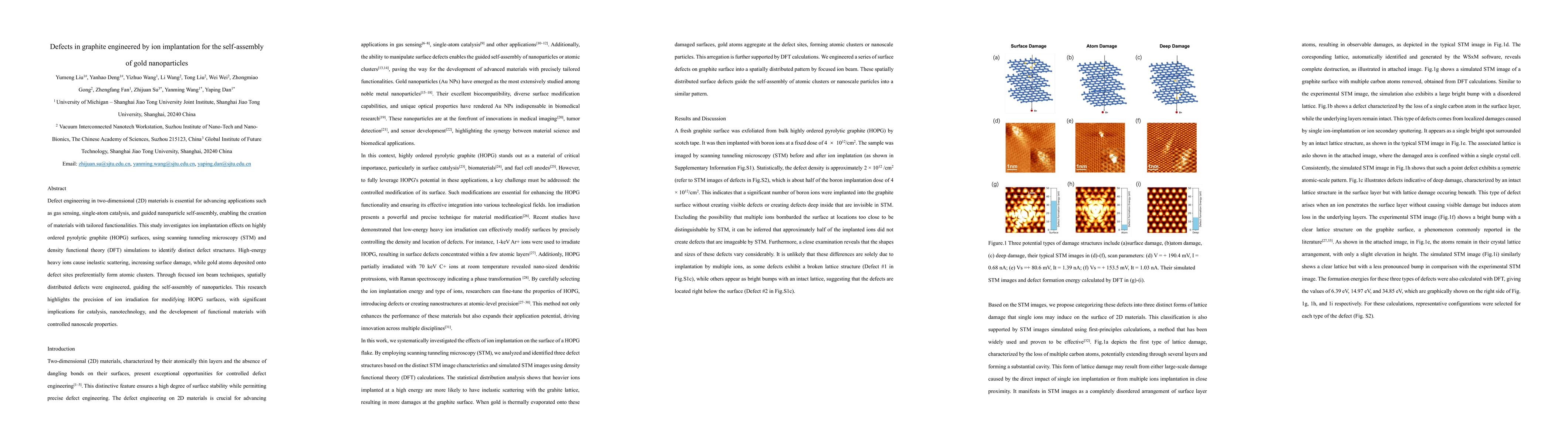
Defect engineering in two-dimensional (2D) materials is essential for advancing applications such as gas sensing, single-atom catalysis, and guided nanoparticle self-assembly, enabling the creation of...
Erbium implanted silicon (Er:Si) is a promising platform for quantum networking applications, but a major obstacle is the formation of multiple Er centres. We show that the previously identified cubic...
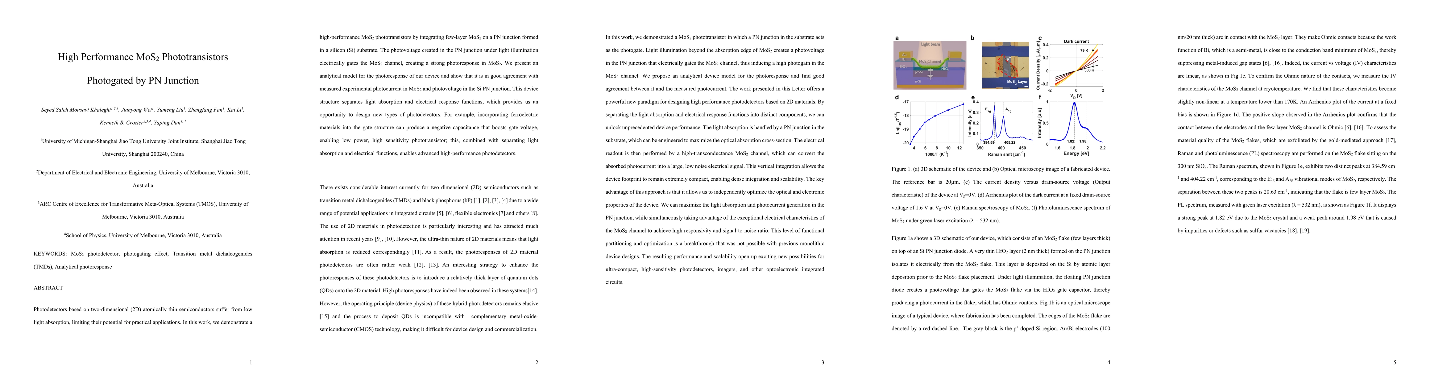
Photodetectors based on two-dimensional (2D) atomically thin semiconductors suffer from low light absorption, limiting their potential for practical applications. In this work, we demonstrate a high-p...
This work demonstrates photon emission gain, i.e., emission of multiple photons per injected electron, through impact excitation in Er-doped silicon light-emitting diodes (LEDs). Conventional methods ...

The primary challenge in silicon photonics is achieving efficient luminescence in the communication band, crucial for its large-scale application. Despite significant efforts, silicon light sources st...
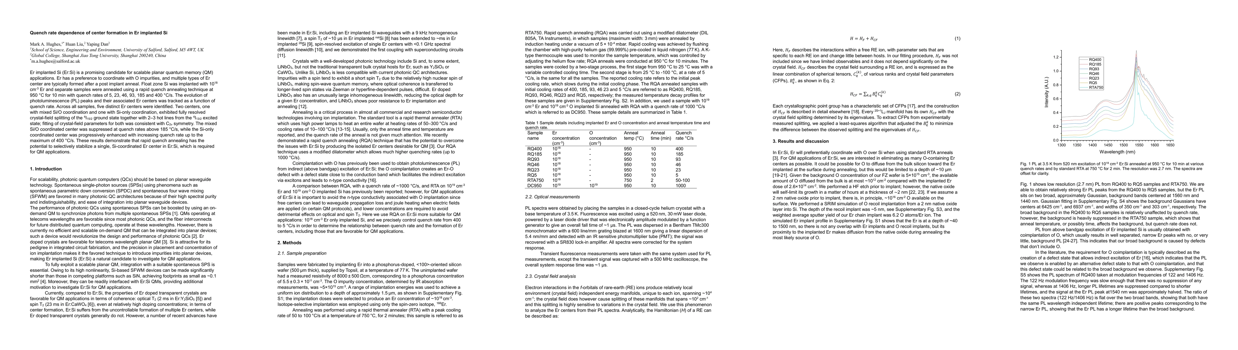
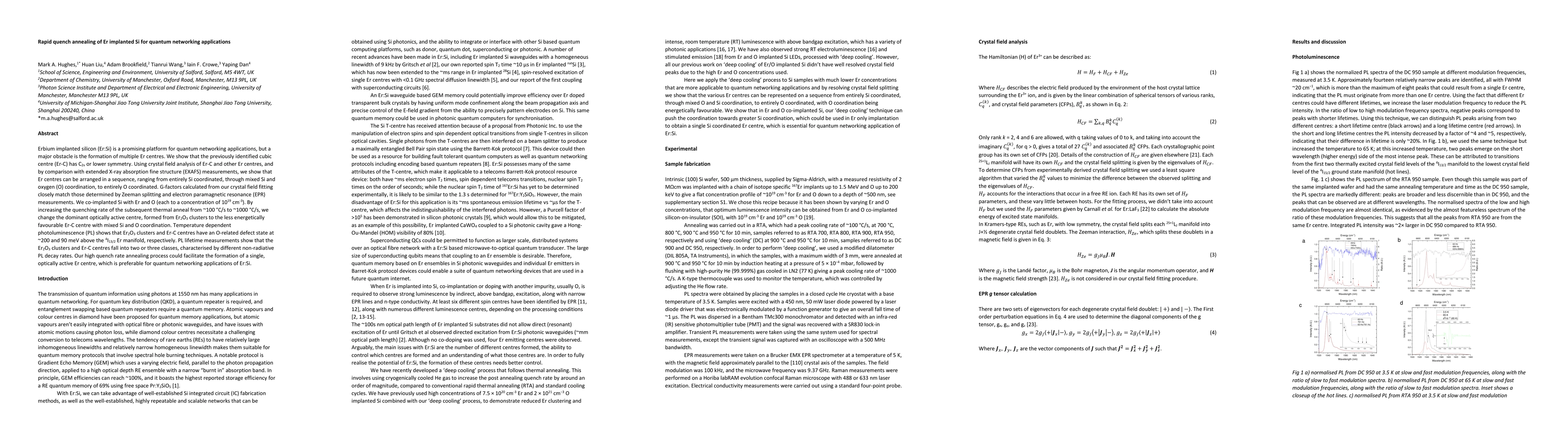
Er implanted Si (Er:Si) is a promising candidate for scalable planar quantum memory (QM) applications. Er has a preference to coordinate with O impurities, and multiple types of Er center are typicall...