This paper presents a technique for real-time optical gas sensing using two-dimensional transition metal dichalcogenides (TMDs) like MoS2, which detects gases such as CO, NO, and NO2 at 10 ppm via charge-transfer-induced photoluminescence changes. The method is supported by density functional theory, potentially advancing remote sensing and lab-on-a-chip technologies.
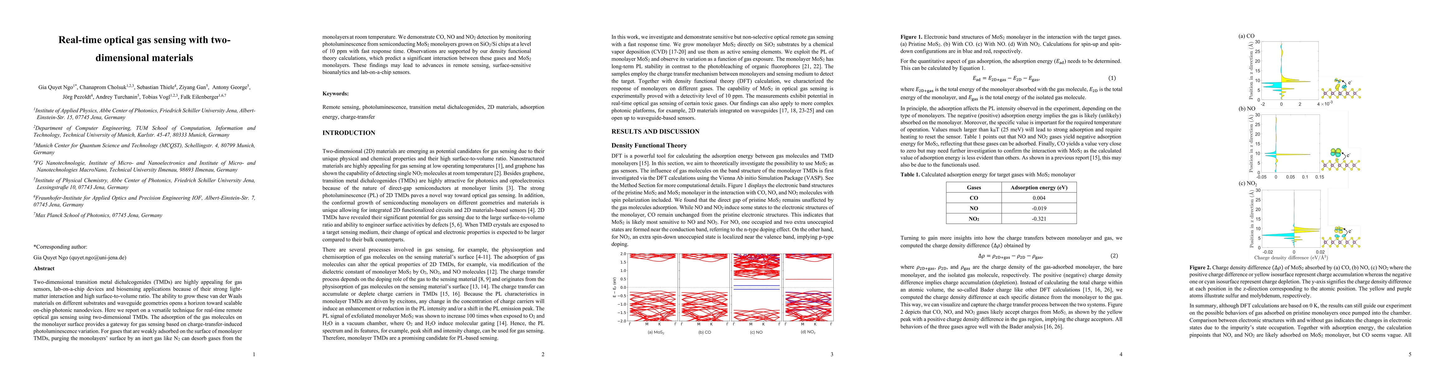
Two-dimensional transition metal dichalcogenides (TMDs) are highly appealing for gas sensors, lab-on-a-chip devices and bio-sensing applications because of their strong light-matter interaction and high surface-to-volume ratio. The ability to grow these van der Waals materials on different substrates and waveguide geometries opens a horizon toward scalable on-chip photonic nanodevices. Here, we report on a versatile technique for real time remote optical gas sensing using two-dimensional TMDs. The adsorption of the gas molecules on the monolayer surface provides a gateway for gas sensing based on charge-transfer-induced photoluminescence variation. For gases that are weakly adsorbed on the surface of monolayer TMDs, purging the monolayers' surface by an inert gas like N2 can desorb gases from the monolayers at room temperature. We demonstrate CO, NO and NO2 detection by monitoring photoluminescence from semiconducting MoS2 monolayers grown on SiO2/Si chips at a level of 10 ppm with fast response time. Observations are supported by our density functional theory calculations, which predict a significant interaction between these gases and MoS2 monolayers. These findings may lead to advances in remote sensing, surface-sensitive bioanalytics and lab-on-a-chip sensors.
Get AI-generated insights about this paper's methodology, results, and significance.
Current paper (gray), citations (green), references (blue)
No similar papers found for this research.
No citations found for this paper.
Title | Authors | Year | Actions |
---|---|---|---|
In-fibre second-harmonic generation with embedded two-dimensional materials
|
Gia Quyet Ngo, Emad Najafidehaghani, Ziyang Gan, Sara Khazaee, M. Siems, A. George, E. Schartner, S. Nolte, H. Ebendorff‐Heidepriem, T. Pertsch, A. Tuniz, M. Schmidt, U. Peschel, A. Turchanin, Falk Eilenberger
|
2022
|
View Paper |
1D p–n Junction Electronic and Optoelectronic Devices from Transition Metal Dichalcogenide Lateral Heterostructures Grown by One‐Pot Chemical Vapor Deposition Synthesis
|
Emad Najafidehaghani, Ziyang Gan, A. George, T. Lehnert, Gia Quyet Ngo, C. Neumann, Tobias Bucher, I. Staude, D. Kaiser, Tobias Vogl, U. Hübner, U. Kaiser, Falk Eilenberger, A. Turchanin
|
2021
|
View Paper |
Integrated Photonics: Scalable Functionalization of Optical Fibers Using Atomically Thin Semiconductors (Adv. Mater. 47/2020)
|
Gia Quyet Ngo, A. George, R. Schock, A. Tuniz, Emad Najafidehaghani, Ziyang Gan, Nils C. Geib, Tobias Bucher, H. Knopf, S. Saravi, C. Neumann, Tilman A. K. Lühder, E. Schartner, S. Warren-Smith, H. Ebendorff‐Heidepriem, T. Pertsch, M. Schmidt, A. Turchanin, Falk Eilenberger
|
2020
|
View Paper |
Scalable Functionalization of Optical Fibers Using Atomically Thin Semiconductors
|
Gia Quyet Ngo, A. George, Robin Tristan Klaus Schock, A. Tuniz, Emad Najafidehaghani, Ziyang Gan, Nils C. Geib, Tobias Bucher, H. Knopf, S. Saravi, C. Neumann, Tilman A. K. Lühder, E. Schartner, S. Warren-Smith, H. Ebendorff‐Heidepriem, T. Pertsch, M. Schmidt, A. Turchanin, Falk Eilenberger
|
2020
|
View Paper |
2D nanostructures beyond graphene: preparation, biocompatibility and biodegradation behaviors.
|
Shige Wang, Xueqing Yang, LingLin Zhou, Jinfeng Li, Hangrong Chen
|
2020
|
View Paper |
Mini-review: Recent progress in the development of MoSe2 based chemical sensors and biosensors
|
Fan Jiang, Wensheng Zhao, Jun Zhang
|
2020
|
View Paper |
Recent advances in two-dimensional-material-based sensing technology toward health and environmental monitoring applications.
|
Deepika Tyagi, Huide Wang, Weichun Huang, Lanping Hu, Yanfeng Tang, Zhinan Guo, Z. Ouyang, Han Zhang
|
2020
|
View Paper |
UV enhanced NO gas sensing properties of the MoS2 monolayer gas sensor
|
S. Ramu, T. Chandrakalavathi, G. Murali, K. S. Kumar, A. Sudharani, M. Ramanadha, Koteswara Rao Peta, R. Jeyalakshmi, R. Vijayalakshmi
|
2019
|
View Paper |
Biocompatibility and biodegradability of 2D materials: graphene and beyond.
|
Cristina Martín, Kostas Kostarelos, M. Prato, A. Bianco
|
2019
|
View Paper |
Controlled growth of transition metal dichalcogenide monolayers using Knudsen-type effusion cells for the precursors
|
A. George, C. Neumann, D. Kaiser, R. Mupparapu, T. Lehnert, U. Hübner, Zian Tang, A. Winter, U. Kaiser, I. Staude, A. Turchanin
|
2019
|
View Paper |
Radiation tolerance of two-dimensional material-based devices for space applications
|
Tobias Vogl, K. Sripathy, Ankur Sharma, P. Reddy, J. Sullivan, J. Machacek, Linglong Zhang, F. Karouta, B. Buchler, M. Doherty, Yuerui Lu, P. Lam
|
2018
|
View Paper |
2D Materials for Gas Sensing Applications: A Review on Graphene Oxide, MoS2, WS2 and Phosphorene
|
M. Donarelli, L. Ottaviano
|
2018
|
View Paper |
Chemical sensing with 2D materials.
|
Cosimo Anichini, Włodzimierz Czepa, Dawid Pakulski, Alessandro Aliprandi, A. Ciesielski, P. Samorí
|
2018
|
View Paper |
The transport and optical sensing properties of MoS2, MoSe2, WS2 and WSe2 semiconducting transition metal dichalcogenides
|
M. Nayeri, M. Moradinasab, M. Fathipour
|
2018
|
View Paper |
Two‐Dimensional Nanostructured Materials for Gas Sensing
|
Xianghong Liu, Tiantian Ma, N. Pinna, Jun Zhang
|
2017
|
View Paper |
Gas sensing in 2D materials
|
Shengxue Yang, Chengbao Jiang, Suhuai Wei
|
2017
|
View Paper |
Nanostructured Materials for Room‐Temperature Gas Sensors
|
Jun Zhang, Xianghong Liu, G. Neri, N. Pinna
|
2016
|
View Paper |
Charge-transfer-based Gas Sensing Using Atomic-layer MoS2
|
B. Cho, M. G. Hahm, Minseok Choi, Jongwon Yoon, A. Kim, Young-Joo Lee, Sung‐Gyu Park, J. Kwon, Chang Su Kim, Myungkwan Song, Y. Jeong, K. Nam, Sangchul Lee, Tae Jin Yoo, C. Kang, B. Lee, Heung Cho Ko, P. Ajayan, Dong-Ho Kim
|
2015
|
View Paper |
High-performance chemical sensing using Schottky-contacted chemical vapor deposition grown monolayer MoS2 transistors.
|
Bilu Liu, Liang Chen, Gang Liu, A. Abbas, M. Fathi, Chongwu Zhou
|
2014
|
View Paper |
Adsorption of gas molecules on monolayer MoS2 and effect of applied electric field
|
Q. Yue, Zhengzheng Shao, Shengli Chang, Jingbo Li
|
2013
|
View Paper |
Broad-range modulation of light emission in two-dimensional semiconductors by molecular physisorption gating.
|
S. Tongay, Jian Zhou, C. Ataca, Jonathan Liu, Jeong Seuk Kang, T. Matthews, Long You, Jingbo Li, J. Grossman, Junqiao Wu
|
2013
|
View Paper |
Fabrication of single- and multilayer MoS2 film-based field-effect transistors for sensing NO at room temperature.
|
Hai Li, Z. Yin, Qiyuan He, H. Li, Xiao Huang, Gang Lu, D. Fam, A. Tok, Qing Zhang, Hua Zhang
|
2012
|
View Paper |
Atomically thin MoS₂: a new direct-gap semiconductor.
|
K. Mak, Changgu Lee, J. Hone, J. Shan, T. Heinz
|
2010
|
View Paper |
Adsorption of Gas Molecules on Graphene Nanoribbons and Its Implication for Nanoscale Molecule Sensor
|
Bing Huang, Zuanyi Li, Zhirong Liu, Gang Zhou, Shaogang Hao, Jian Wu, B. Gu, W. Duan
|
2008
|
View Paper |
Detection of individual gas molecules adsorbed on graphene.
|
F. Schedin, A.K. Geim, S. Morozov, E. Hill, P. Blake, M. Katsnelson, K. Novoselov
|
2006
|
View Paper |
From ultrasoft pseudopotentials to the projector augmented-wave method
|
G. Kresse, D. Joubert
|
1999
|
View Paper |
Generalized Gradient Approximation Made Simple.
|
J. Perdew, K. Burke, M. Ernzerhof
|
1996
|
View Paper |
Efficient iterative schemes for ab initio total-energy calculations using a plane-wave basis set.
|
G. Kresse, J. Furthmüller
|
1996
|
View Paper |
Efficiency of ab-initio total energy calculations for metals and semiconductors using a plane-wave basis set
|
G. Kresse, J. Furthmüller
|
1996
|
View Paper |
Projector augmented-wave method.
|
P. Blöchl
|
1994
|
View Paper |
SPECIAL POINTS FOR BRILLOUIN-ZONE INTEGRATIONS
|
H. Monkhorst, J. Pack
|
1976
|
View Paper |
A highly sensitive chemical gas detecting transistor based on highly crystalline CVD-grown MoSe2 films
|
J. Baek, Demin Yin, Na Liu, I. Omkaram, Chulseung Jung, Healin Im, Seongin Hong, Seung Min Kim, Y. Hong, Jaehyun Hur, Y. Yoon, Sunkook Kim
|
2016
|
View Paper |
A First-Principles Investigation of Various Gas (CO, H 2 O, NO, and O 2 ) Absorptions on a WS 2 Monolayer: Stability and Electronic Properties
|
2015
|
||
Gas Adsorption on MoS 2 Monolayer from First-Principles Calculations
|
2014
|
||
Direct growth of monolayer MoS 2 on nanostructured silicon
|
|||
Institute of Applied Physics, Abbe Center of Photonics, Friedrich Schiller University Jena
|
|||
Department of Computer Engineering, TUM School of Computation, Information and Technology, Technical University of Munich, Karlstr. 45-47, 80333 Munich, Germany
|
|||
Gia Quyet Ngo 1* , Chanaprom Cholsuk 1,2,3 , Sebastian Thiele 4 , Ziyang Gan 5 , Antony George 5 , Jörg Pezoldt 4 , Andrey Turchanin 5 , Tobias Vogl 1,2,3
|
|||
Institute of Physical Chemistry, Abbe Center
|
Showing first page preview. Click "Open Full PDF" to view the complete paper.
Your comment contains inappropriate language and has been rejected.
Are you sure you want to remove this tag? This action cannot be undone.
Someone just favorited a paper!
Comments (0)