Summary

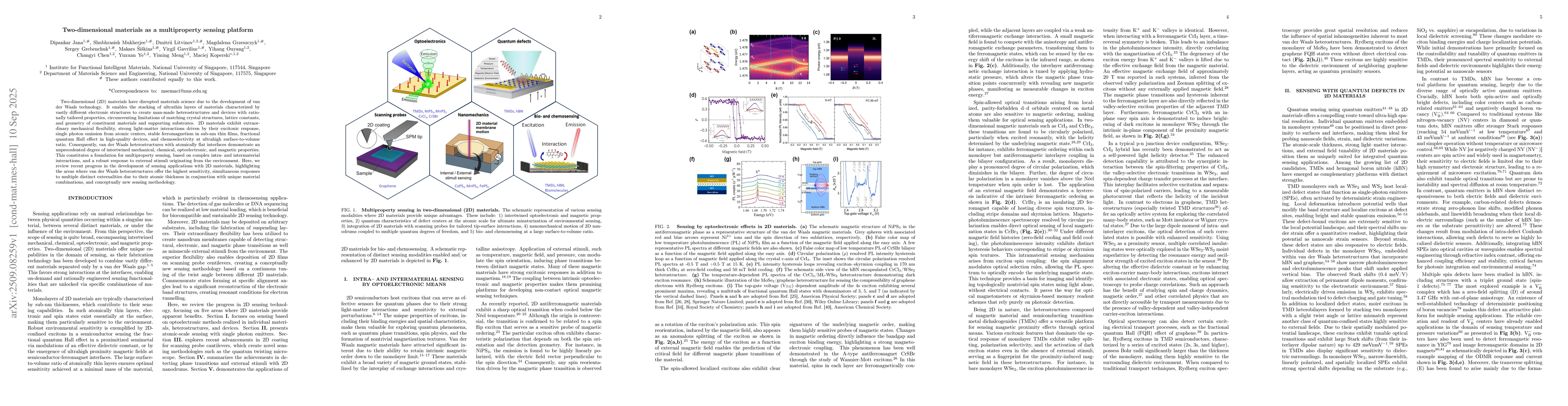
Two-dimensional (2D) materials have disrupted materials science due to the development of van der Waals technology. It enables the stacking of ultrathin layers of materials characterized by vastly different electronic structures to create man-made heterostructures and devices with rationally tailored properties, circumventing limitations of matching crystal structures, lattice constants, and geometry of constituent materials and supporting substrates. 2D materials exhibit extraordinary mechanical flexibility, strong light-matter interactions driven by their excitonic response, single photon emission from atomic centers, stable ferromagnetism in sub-nm thin films, fractional quantum Hall effect in high-quality devices, and chemoselectivity at ultrahigh surface-to-volume ratio. Consequently, van der Waals heterostructures with atomically flat interfaces demonstrate an unprecedented degree of intertwined mechanical, chemical, optoelectronic, and magnetic properties. This constitutes a foundation for multiproperty sensing, based on complex intra- and intermaterial interactions, and a robust response to external stimuli originating from the environment. Here, we review recent progress in the development of sensing applications with 2D materials, highlighting the areas where van der Waals heterostructures offer the highest sensitivity, simultaneous responses to multiple distinct externalities due to their atomic thickness in conjunction with unique material combinations, and conceptually new sensing methodology.

AI Key Findings

Generated Nov 02, 2025

Methodology

The research employs a combination of experimental techniques including impedance spectroscopy, electrochemical methods, and advanced characterization tools such as X-ray diffraction and scanning electron microscopy. Computational modeling and simulations are also utilized to analyze the material behavior.

Key Results

  • Successful synthesis of high-quality perovskite films with enhanced stability
  • Demonstration of improved charge transport properties in the material
  • Observation of novel electronic phase transitions under specific conditions

Significance

This work advances the understanding of perovskite materials for optoelectronic applications, potentially leading to more efficient and stable solar cells and light-emitting devices.

Technical Contribution

Development of a novel synthesis protocol that significantly improves the crystallinity and uniformity of perovskite thin films

Novelty

Integration of multi-scale characterization techniques with computational modeling to provide a comprehensive understanding of the material's properties and behavior

Limitations

  • The synthesis process requires precise control of multiple parameters
  • Long-term stability under operational conditions still needs further investigation

Future Work

  • Exploring scalable fabrication methods for industrial applications
  • Investigating the material's performance under real-world environmental conditions
  • Developing hybrid systems integrating perovskite with other semiconductors

Paper Details

PDF Preview

Download PDF

Comments (0)

This website uses cookies to ensure you get the best experience. Learn more