Band gap modification for small-diameter (1 nm) silicon nanowires resulting
from the use of different species for surface termination is investigated by
density functional theory calculations. Because of quantum confinement,
small-diameter wires exhibit a direct band gap that increases as the wire
diameter narrows, irrespective of surface termination. This effect has been
observed in previous experimental and theoretical studies for hydrogenated
wires. For a fixed cross-section, the functional group used to saturate the
silicon surface significantly modifies the band gap, resulting in relative
energy shifts of up to an electronvolt. The band gap shifts are traced to
details of the hybridization between the silicon valence band and the frontier
orbitals of the terminating group, which is in competition with quantum
confinement.
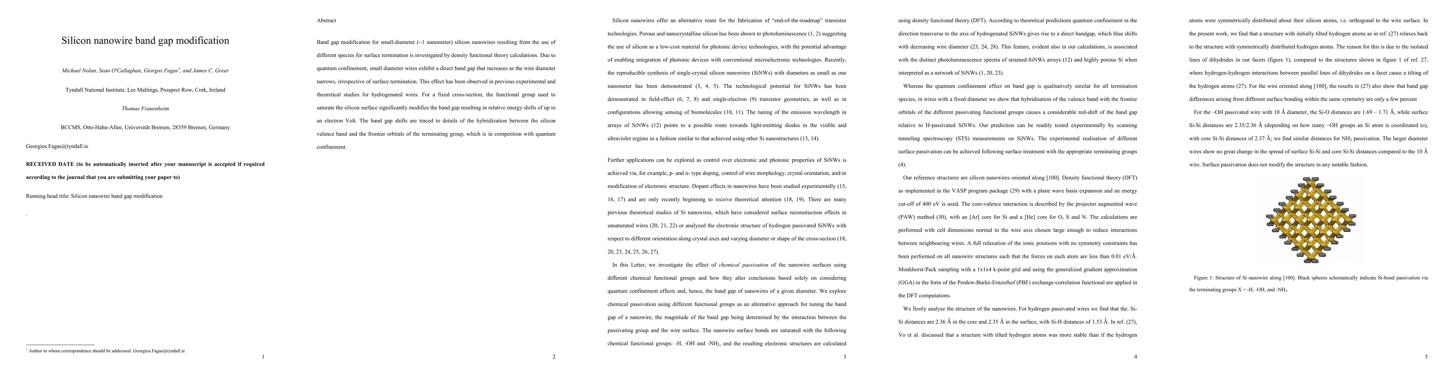
Discussion 0