The paper develops a framework to link density functional theory calculations of electronic band structures with chemical bonding in materials, specifically explaining the indirect band gap in silicon. This approach provides new insights into silicon’s conduction band minimum, which is crucial for its applications in photovoltaics and electronics.
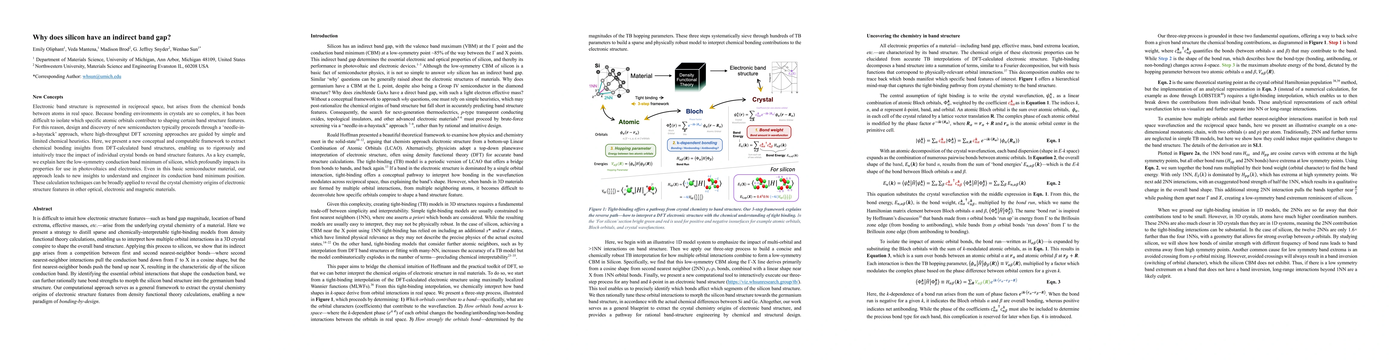
Density functional theory (DFT) is a powerful tool for predicting the electronic band structures of functional materials. However, it is often difficult to intuit how major band structure features$-$such as band gap magnitude, location of band extrema, effective masses, etc.$-$arise from the underlying crystal chemistry of a material. Band structure is represented in reciprocal space, but arises from the orbital and bonding interactions between atoms in real space. Here, we present a conceptual and computable framework to extract chemical bonding origins of DFT-calculated band structure features. As a key example, we explain here the indirect band gap of silicon, which profoundly impacts its properties for use in photovoltaics and electronics. Even in this basic semiconductor material, our approach leads to new insights to understand and engineer its conduction band minimum position. These calculation techniques can be broadly applied to reveal the crystal chemistry origins of electronic structure features in other optical, electronic, and magnetic materials.
Generated Sep 07, 2025
The research presents a conceptual and computable framework to extract chemical bonding origins of DFT-calculated band structures, focusing on explaining silicon's indirect band gap. This involves a three-step process: determining orbital character, bond shape in k-space, and strength of hopping parameters.
This research is significant as it provides new insights into understanding and engineering the conduction band minimum position in silicon, a fundamental material for photovoltaics and electronics. The framework can be broadly applied to reveal the crystal chemistry origins of electronic structure features in other materials.
The paper introduces a three-step process linking chemical bonding to band structure, resulting in a sparse and interpretable tight-binding model that helps understand the crystal chemistry origins of band structure features.
The work offers a novel approach by systematically connecting bonding interactions to band structure, providing a clear physical mechanism for silicon's indirect band gap, and demonstrating the potential for materials design through 'bonding-by-design'.
Current paper (gray), citations (green), references (blue)
Display is limited for performance on very large graphs.
Title | Authors | Year | Actions |
---|
Comments (0)