This paper demonstrates simultaneous quantisation of both conduction and valence band states in silicon using ultra-shallow, high-density phosphorus doping profiles. The study reveals that the confinement of VB states between the P dopant layer and Si surface allows independent control over conduction and valence band quantisation properties.
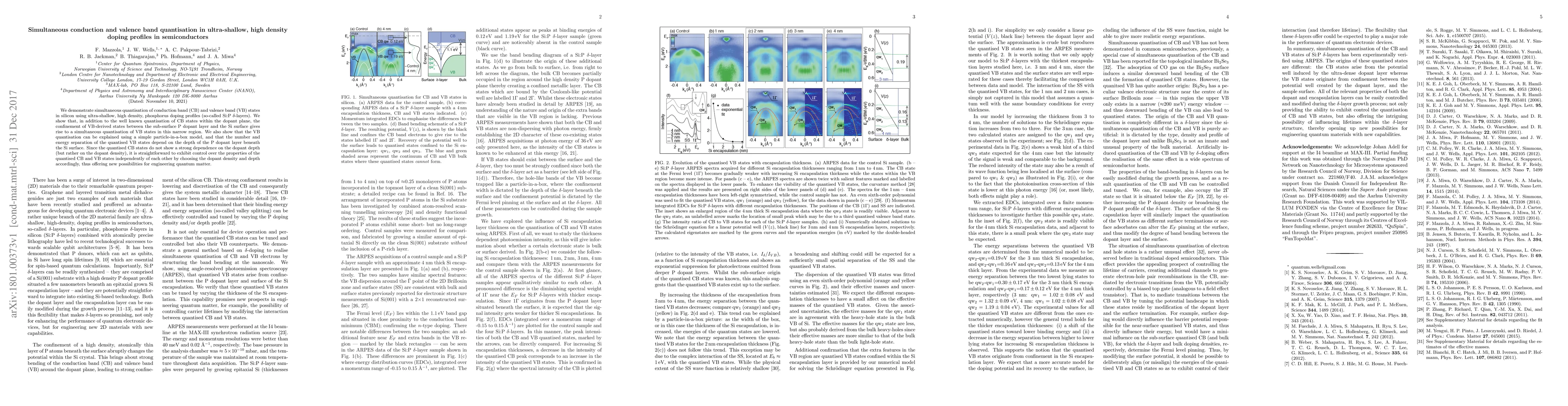
We demonstrate simultaneous quantisation of conduction band (CB) and valence band (VB) states in silicon using ultra-shallow, high density, phosphorus doping profiles (so-called Si:P $\delta$-layers). We show that, in addition to the well known quantisation of CB states within the dopant plane, the confinement of VB-derived states between the sub-surface P dopant layer and the Si surface gives rise to a simultaneous quantisation of VB states in this narrow region. We also show that the VB quantisation can be explained using a simple particle-in-a-box model, and that the number and energy separation of the quantised VB states depend on the depth of the P dopant layer beneath the Si surface. Since the quantised CB states do not show a strong dependence on the dopant depth (but rather on the dopant density), it is straightforward to exhibit control over the properties of the quantised CB and VB states independently of each other by choosing the dopant density and depth accordingly, thus offering new possibilities for engineering quantum matter.
This graph shows how this paper is connected to other research. The current paper is shown in dark gray, papers that cite it are in green, and papers it references are in blue. You can:
• Hover over any node to see the paper title
• Click a node to view that paper's details
• Drag nodes to rearrange the graph
• Use the zoom controls (bottom right) to zoom in/out
Title | Authors | Year | Actions |
---|---|---|---|
Direct Observation of 2DEG States in Shallow Si:Sb δ-Layers
|
F. Strand, S. Cooil, Quinn T. Campbell, John J. Flounders, H. Røst, A. C. Åsland, Alv Johan Skarpeid, Marte P. Stalsberg, Jinbang Hu, J. Bakkelund, V. Bjelland, A. Preobrajenski, Zheshen Li, M. Bianchi, J. Miwa, J. Wells
|
2024
|
View Paper |
Momentum‐Space Imaging of Ultra‐Thin Electron Liquids in δ‐Doped Silicon
|
Procopios Constantinou, T. Stock, E. Crane, A. Kölker, M. V. van Loon, Juerong Li, S. Fearn, Henric Bornemann, N. D'Anna, A. Fisher, V. Strocov, G. Aeppli, N. Curson, S. R. Schofield
|
2023
|
View Paper |
Electronic structure of boron and aluminum δ-doped layers in silicon
|
Q. Campbell, S. Misra, A. Baczewski
|
2023
|
View Paper |
Robust behavior and spin-texture stability of the topological surface state in Bi2Se3 upon deposition of gold
|
O. J. Clark, F. Freyse, L. Yashina, O. Rader, J. Sánchez-Barriga
|
2022
|
View Paper |
Revealing quantum effects in highly conductive δ-layer systems
|
D. Mamaluy, J. P. Mendez, Xujiao Gao, S. Misra
|
2021
|
View Paper |
Revealing quantum effects in highly conductive δ-layer systems
|
D. Mamaluy, J. P. Mendez, Xujiao Gao, S. Misra
|
2021
|
View Paper |
The sub-band structure of atomically sharp dopant profiles in silicon
|
F. Mazzola, Chin-Yi Chen, R. Rahman, Xiegang Zhu, C. Polley, T. Balasubramanian, P. King, P. Hofmann, J. Miwa, J. Wells
|
2020
|
View Paper |
The occupied electronic structure of ultrathin boron doped diamond
|
Alex Schenk, A. Pakpour-Tabrizi, A. J. Holt, S. Mahatha, Fabian Arnold, M. Bianchi, Richard B Jackman, J. A. Miwa, Ph. Hofmann, S. Cooil, J. Wells, Federico Mazzola
|
2019
|
View Paper |
The sub-band structure of atomically sharp dopant profiles in silicon
|
F. Mazzola, Chin-Yi Chen, R. Rahman, Xiegang Zhu, C. Polley, T. Balasubramanian, P. King, P. Hofmann, J. Miwa, J. Wells
|
2019
|
View Paper |
Comments (0)