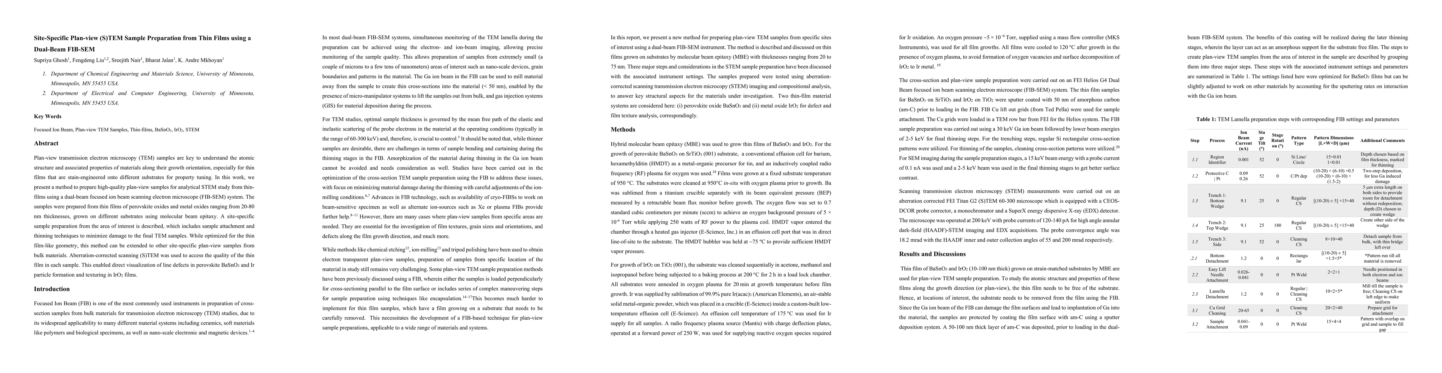
Site-Specific Plan-view (S)TEM Sample Preparation from Thin Films using a Dual-Beam FIB-SEM
Publication
Metrics
AI Quick Summary
This paper presents a method for preparing high-quality plan-view TEM samples from thin films using a dual-beam FIB-SEM system, enabling site-specific analysis of perovskite and metal oxide films. The method minimizes damage and allows for direct visualization of defects in materials like BaSnO3 and IrO2.
Paper Preview
Abstract
Plan-view transmission electron microscopy (TEM) samples are key to understand the atomic structure and associated properties of materials along their growth orientation, especially for thin films that are stain-engineered onto different substrates for property tuning. In this work, we present a method to prepare high-quality plan-view samples for analytical STEM study from thin-films using a dual-beam focused ion beam scanning electron microscope (FIB-SEM) system. The samples were prepared from thin films of perovskite oxides and metal oxides ranging from 20-80 nm thicknesses, grown on different substrates using molecular beam epitaxy. A site-specific sample preparation from the area of interest is described, which includes sample attachment and thinning techniques to minimize damage to the final TEM samples. While optimized for the thin film-like geometry, this method can be extended to other site-specific plan-view samples from bulk materials. Aberration-corrected scanning (S)TEM was used to access the quality of the thin film in each sample. This enabled direct visualization of line defects in perovskite BaSnO3 and Ir particle formation and texturing in IrO2 films.
AI Key Findings
Get AI-generated insights about this paper's methodology, results, significance, and more — seven facets brought into focus.
Impact
Paper Details
Authors
PDF Preview
Key Terms
Citation Network
Current paper (gray), citations (green), references (blue)
Display is limited for performance on very large graphs.
Discussion 0