Spontaneous Transition from Conformal to Two-Dimensional Growth in Ge/GeSn Core/Shell Nanowires
Publication
Metrics
Paper Preview
Abstract
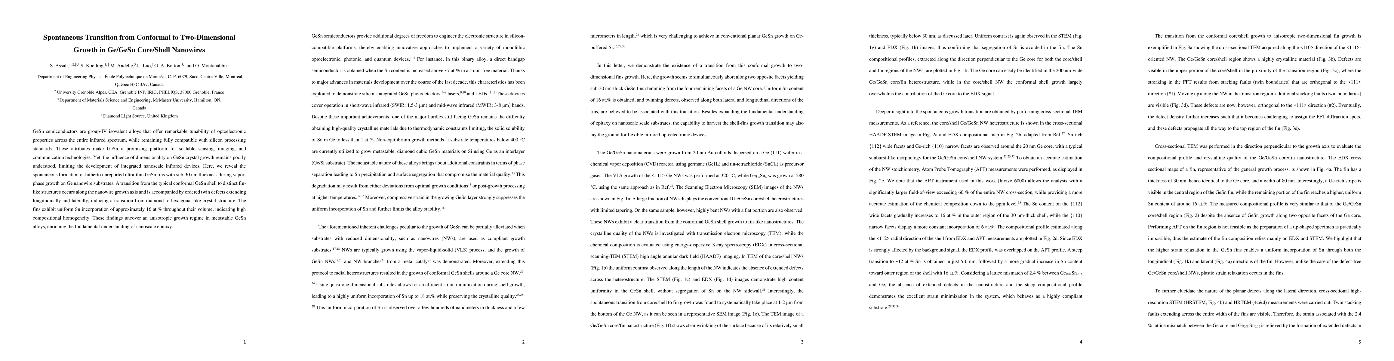
GeSn semiconductors are group-IV isovalent alloys that offer remarkable tunability of optoelectronic properties across the entire infrared spectrum, while remaining fully compatible with silicon processing standards. These attributes make GeSn a promising platform for scalable sensing, imaging, and communication technologies. Yet, the influence of dimensionality on GeSn crystal growth remains poorly understood, limiting the development of integrated nanoscale infrared devices. Here, we reveal the spontaneous formation of hitherto unreported ultra-thin GeSn fins with sub-30 nm thickness during vapor-phase growth on Ge nanowire substrates. A transition from the typical conformal GeSn shell to distinct fin-like structures occurs along the nanowire growth axis and is accompanied by ordered twin defects extending longitudinally and laterally, inducing a transition from diamond to hexagonal-like crystal structure. The fins exhibit uniform Sn incorporation of approximately 16 at.% throughout their volume, indicating high compositional homogeneity. These findings uncover an anisotropic growth regime in metastable GeSn alloys, enriching the fundamental understanding of nanoscale epitaxy.
AI Key Findings
Get AI-generated insights about this paper's methodology, results, significance, and more — seven facets brought into focus.
Discussion 0