Strain engineering in semiconducting two-dimensional crystals
Publication
Metrics
AI Quick Summary
This paper reviews recent advances in strain engineering of semiconducting two-dimensional crystals, focusing on manipulating their optical and electronic properties through controlled elastic strain. Special emphasis is placed on transition metal dichalcogenides, while also considering other materials like black phosphorus and silicene, and discussing potential applications in nanoelectronics and optoelectronics.
Paper Preview
Abstract
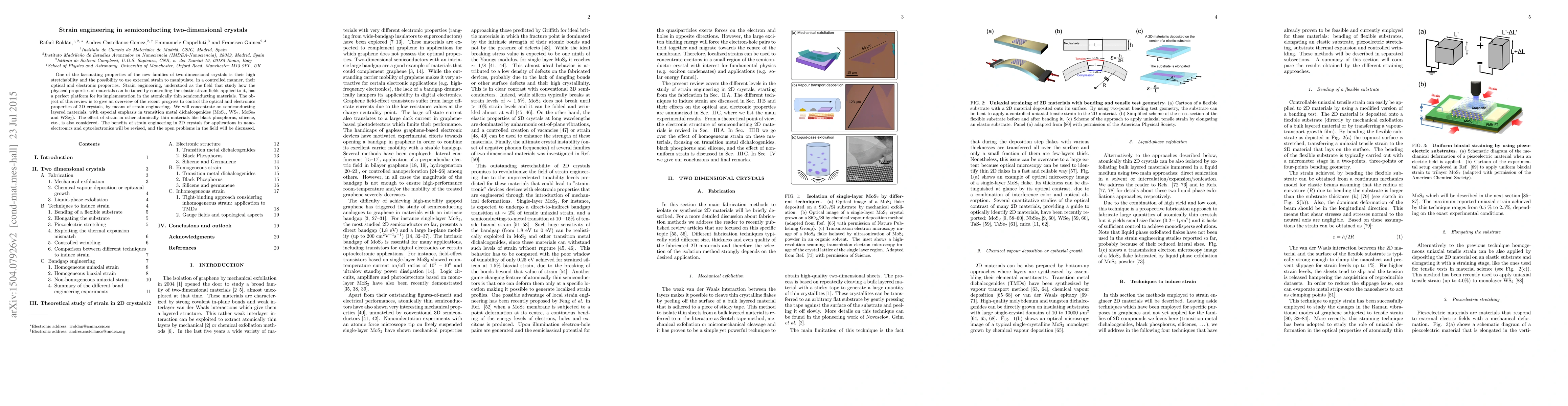
One of the fascinating properties of the new families of two-dimensional crystals is their high stretchability and the possibility to use external strain to manipulate, in a controlled manner, their optical and electronic properties. Strain engineering, understood as the field that study how the physical properties of materials can be tuned by controlling the elastic strain fields applied to it, has a perfect platform for its implementation in the atomically thin semiconducting materials. The object of this review is to give an overview of the recent progress to control the optical and electronics properties of 2D crystals, by means of strain engineering. We will concentrate on semiconducting layered materials, with especial emphasis in transition metal dichalcogenides (MoS$_2$, WS$_2$, MoSe$_2$ and WSe$_2$). The effect of strain in other atomically thin materials like black phosphorus, silicene, etc., is also considered. The benefits of strain engineering in 2D crystals for applications in nanoelectronics and optoelectronics will be revised, and the open problems in the field will be discussed.
AI Key Findings
Get AI-generated insights about this paper's methodology, results, significance, and more — seven facets brought into focus.
Impact
Paper Details
PDF Preview
Key Terms
Citation Network
Current paper (gray), citations (green), references (blue)
Display is limited for performance on very large graphs.
Discussion 0