Super-resolution Imaging by Evanescent Wave Coupling to Surface States on Effective Gain Media
1206.4148
Published Jun 20, 2012
Publication
Published:
Jun 20, 2012
Updated:
Jun 02, 2025
Categories:
physics.optics
Metrics
Source:
ArXiv
Paper Preview
Abstract
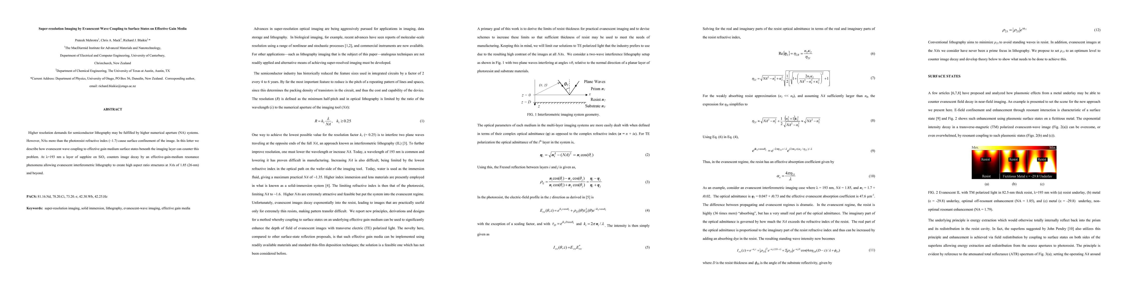
Higher resolution demands for semiconductor lithography may be fulfilled by higher numerical aperture (NA) systems. However, NAs more than the photoresist refractive index (~1.7) cause surface confinement of the image. In this letter we describe how evanescent wave coupling to effective gain medium surface states beneath the imaging layer can counter this problem. At {\lambda}=193 nm a layer of sapphire on SiO2 counters image decay by an effective-gain-medium resonance phenomena allowing evanescent interferometric lithography to create high aspect ratio structures at NAs of 1.85 (26-nm) and beyond.
AI Key Findings
Get AI-generated insights about this paper's methodology, results, significance, and more — seven facets brought into focus.
Impact
1
References
Paper Details
Paper ID:
1206.4148
License:
http://arxiv.org/licenses/nonexclusive-distrib/1.0/
Categories:
physics.optics
PDF Preview
Key Terms
nm
(0.278)
gain
(0.266)
medium
(0.248)
layer
(0.224)
image
(0.209)
refractive
(0.205)
surface
(0.196)
na
(0.191)
Discussion 0