Authors
Summary
Thermal scanning probe lithography offers high resolution and versatility, making it a promising alternative for fabricating photonic devices. Here, we introduce a new method that expands its applications by enabling direct fabrication of arbitrary perforated patterns on a silver film.
AI Key Findings
Generated Oct 30, 2025
Methodology
The research employs thermal scanning probe lithography (t-SPL) to fabricate perforated patterns on silver films. It involves a bilayer lift-off configuration, thermal resist sublimation, and wet etching of metallic films. The process includes sample preparation, metal deposition, resist coating, lithography, etching, and lift-off steps.
Key Results
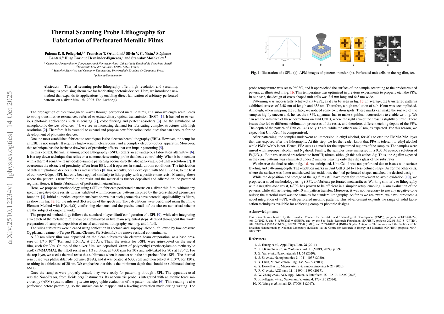
- Successful fabrication of cross-shaped perforated patterns on silver films with sub-10 nm resolution.
- Achieved high-resolution patterning with average cross dimensions of 2.48 µm in length and 638 nm in width.
- Demonstrated the feasibility of creating perforated metallic films without the need for negative-tone resists.
Significance
This research advances photonic device fabrication by enabling high-resolution, direct patterning of complex perforated structures on metallic films. It offers a simpler, room-temperature alternative to electron-beam lithography, expanding possibilities for nanophotonic applications.
Technical Contribution
Introduces a novel t-SPL methodology for fabricating perforated metallic films without negative-tone resists, integrating wet etching and bilayer lift-off techniques.
Novelty
The work presents the first use of t-SPL for direct fabrication of arbitrary perforated patterns on metallic films, eliminating the need for negative-tone resists and enabling complex photonic structures.
Limitations
- Surface oxidation issues caused unevenness, affecting pattern accuracy and requiring significant leveling corrections.
- Variability in etching depths due to sublimation differences, leading to inconsistent perforation depths across unit cells.
Future Work
- Improving Ag film deposition and storage techniques to minimize oxidation.
- Exploring the application of these perforated structures in infrared filters and other photonic devices.
- Refining the numerical simulation methods for better prediction of optical transmission properties.
Paper Details
PDF Preview
Similar Papers
Found 5 papersQuantitative mapping of smooth topographic landscapes produced by thermal scanning-probe lithography
Peter Bøggild, Søren Raza, Timothy J. Booth et al.
Mechanical scanning probe lithography of perovskites for fabrication of high-Q planar polaritonic cavities
P. Alekseev, N. Glebov, M. Masharin et al.
Strained 2D TMD lateral heterojunctions via grayscale thermal-Scanning Probe Lithography
F. Caglieris, M. Ceccardi, M. C. Giordano et al.
Sub 20 nm Silicon Patterning and Metal Lift-Off Using Thermal Scanning Probe Lithography
James L. Hedrick, Heiko Wolf, Armin W. Knoll et al.
Comments (0)