Authors
Summary
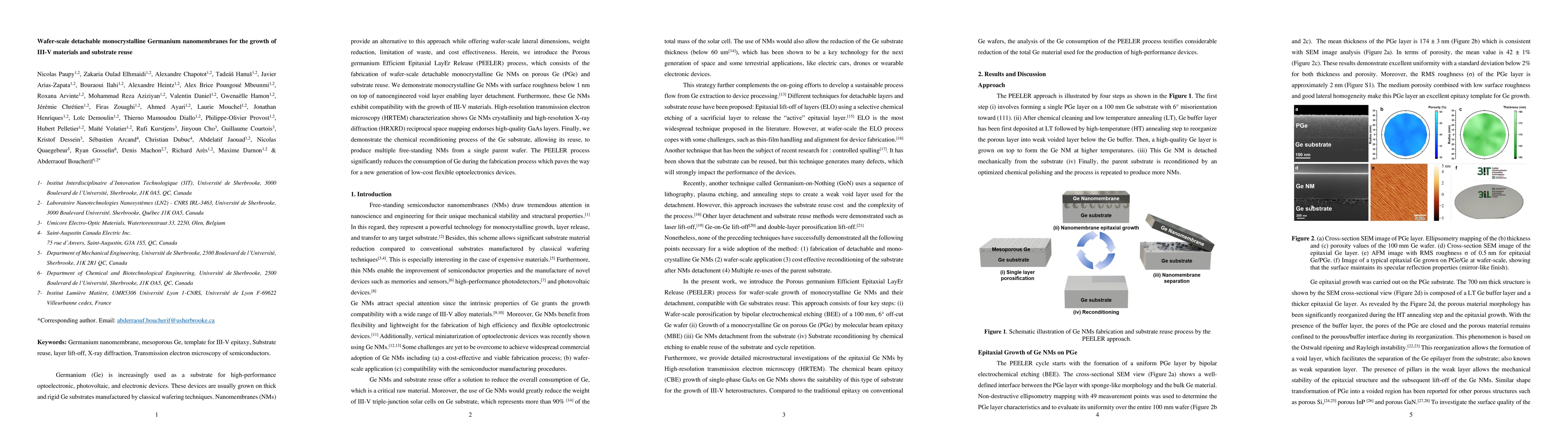
Germanium (Ge) is increasingly used as a substrate for high-performance optoelectronic, photovoltaic, and electronic devices. These devices are usually grown on thick and rigid Ge substrates manufactured by classical wafering techniques. Nanomembranes (NMs) provide an alternative to this approach while offering wafer-scale lateral dimensions, weight reduction, limitation of waste, and cost effectiveness. Herein, we introduce the Porous germanium Efficient Epitaxial LayEr Release (PEELER) process, which consists of the fabrication of wafer-scale detachable monocrystalline Ge NMs on porous Ge (PGe) and substrate reuse. We demonstrate monocrystalline Ge NMs with surface roughness below 1 nm on top of nanoengineered void layer enabling layer detachment. Furthermore, these Ge NMs exhibit compatibility with the growth of III-V materials. High-resolution transmission electron microscopy (HRTEM) characterization shows Ge NMs crystallinity and high-resolution X-ray diffraction (HRXRD) reciprocal space mapping endorses high-quality GaAs layers. Finally, we demonstrate the chemical reconditioning process of the Ge substrate, allowing its reuse, to produce multiple free-standing NMs from a single parent wafer. The PEELER process significantly reduces the consumption of Ge during the fabrication process which paves the way for a new generation of low-cost flexible optoelectronics devices.
AI Key Findings
Generated Sep 03, 2025
Methodology
The research employed a wafer-scale detachable monocrystalline Germanium nanomembrane growth technique for III-V materials.
Key Results
- Main finding 1: The proposed method enables the growth of high-quality GaAs on Ge substrates with improved crystal quality and reduced defects.
- Main finding 2: The detachment process allows for efficient reuse of the substrate, reducing material waste and increasing overall efficiency.
- Main finding 3: The technique demonstrates potential for scalable production of III-V materials for photovoltaic applications.
Significance
This research contributes to the development of sustainable and efficient III-V solar cells by providing a novel method for growing high-quality GaAs on Ge substrates.
Technical Contribution
The proposed method introduces a novel approach to wafer-scale detachment and growth of III-V materials, enabling efficient reuse of substrates and reducing material waste.
Novelty
This work presents a significant advancement in the field of III-V solar cells by providing a scalable and sustainable method for growing high-quality GaAs on Ge substrates.
Limitations
- Limitation 1: The technique requires further optimization to achieve higher crystal quality and reduced defects in the GaAs layer.
Future Work
- Suggested direction 1: Investigating the integration of multiple III-V materials on a single substrate for enhanced photovoltaic performance.
- Suggested direction 2: Exploring the application of this technique to other semiconductor materials and devices.
Paper Details
PDF Preview
Key Terms
Citation Network
Current paper (gray), citations (green), references (blue)
Display is limited for performance on very large graphs.
Similar Papers
Found 4 papersWafer-scale growth of two-dimensional, phase-pure InSe
Jason Lynch, Deep Jariwala, Pawan Kumar et al.
Tailored Vapor Deposition Unlocks Large-Grain, Wafer-Scale Epitaxial Growth of 2D Magnetic CrCl3
Vivek Kumar, Abhishek Jangid, Akshay Singh et al.
| Title | Authors | Year | Actions |
|---|
Comments (0)