$WSe_2$ as transparent top gate for near-field experiments
Publication
Metrics
AI Quick Summary
Researchers demonstrate that few-layer WSe2 can be used as a transparent top gate electrode in infrared near-field microscopy, enabling the tuning of plasmon wavelength and extraction of energy gap values.
Paper Preview
Abstract
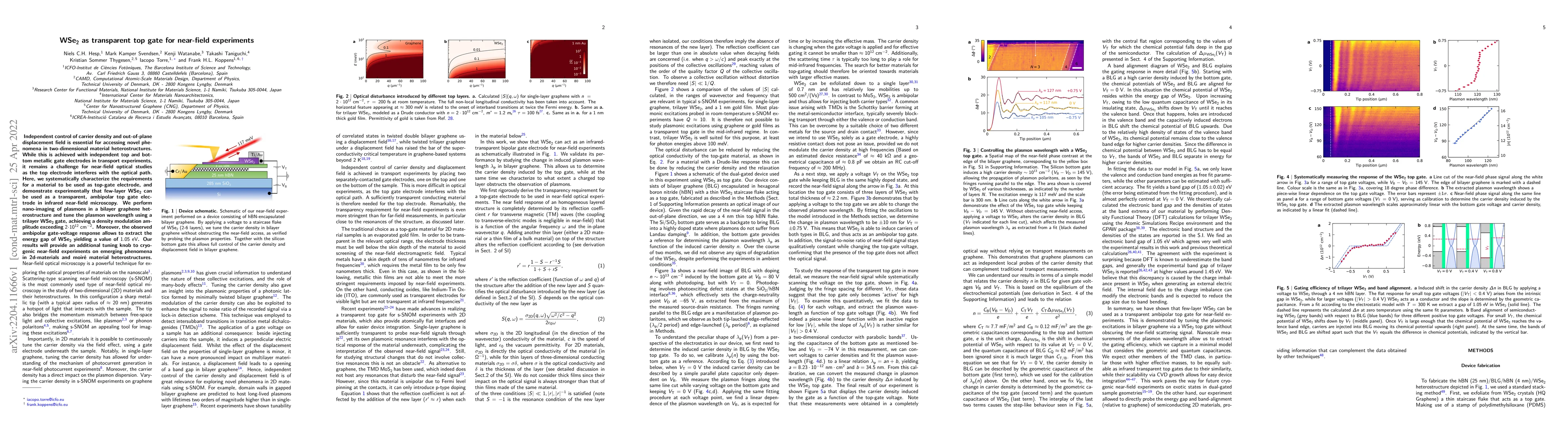
Independent control of carrier density and out-of-plane displacement field is essential for accessing novel phenomena in two-dimensional material heterostructures. While this is achieved with independent top and bottom metallic gate electrodes in transport experiments, it remains a challenge for near-field optical studies as the top electrode interferes with the optical path. Here, we systematically characterize the requirements for a material to be used as top-gate electrode, and demonstrate experimentally that few-layer WSe_2 can be used as a transparent, ambipolar top gate electrode in infrared near-field microscopy. We perform nano-imaging of plasmons in a bilayer graphene heterostructure and tune the plasmon wavelength using a trilayer WSe_2 gate, achieving a density modulation amplitude exceeding 2 10^{12} cm^{-2}. Moreover, the observed ambipolar gate-voltage response allows to extract the energy gap of WSe_2 yielding a value of 1.05 eV. Our results will provide an additional tuning knob to cryogenic near-field experiments on emerging phenomena in two-dimensional materials and moir\'e material heterostructures.
AI Key Findings
Get AI-generated insights about this paper's methodology, results, significance, and more — seven facets brought into focus.
Impact
Paper Details
Authors
PDF Preview
Key Terms
Citation Network
Current paper (gray), citations (green), references (blue)
Display is limited for performance on very large graphs.
Discussion 0