Academic Profile
Statistics
Similar Authors
Papers on arXiv
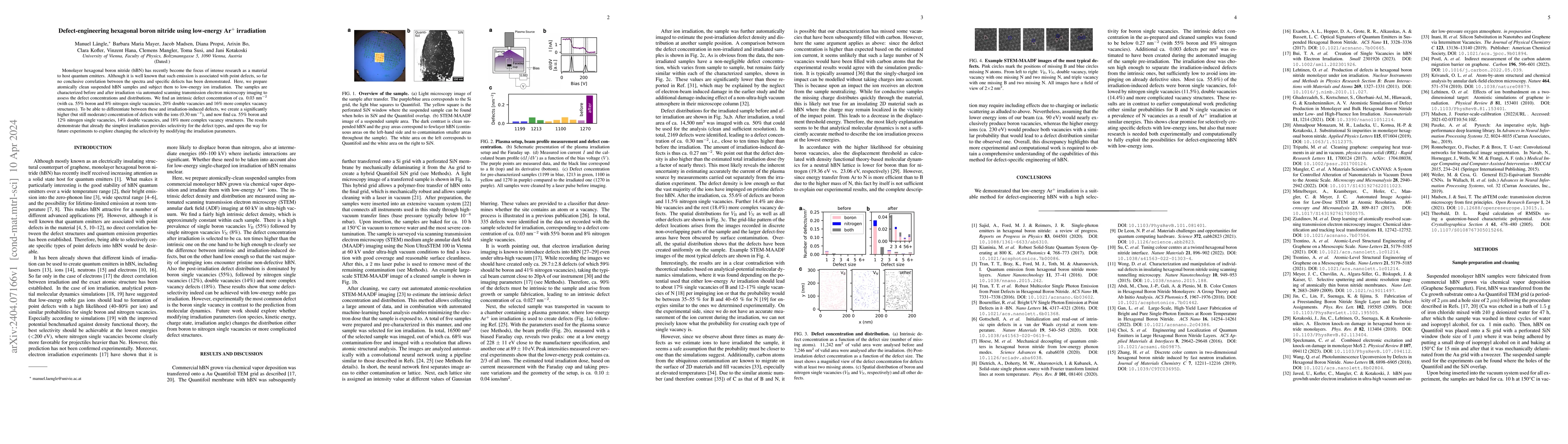
Monolayer hexagonal boron nitride (hBN) has recently become the focus of intense research as a material to host quantum emitters. Although it is well known that such emission is associated with poin...
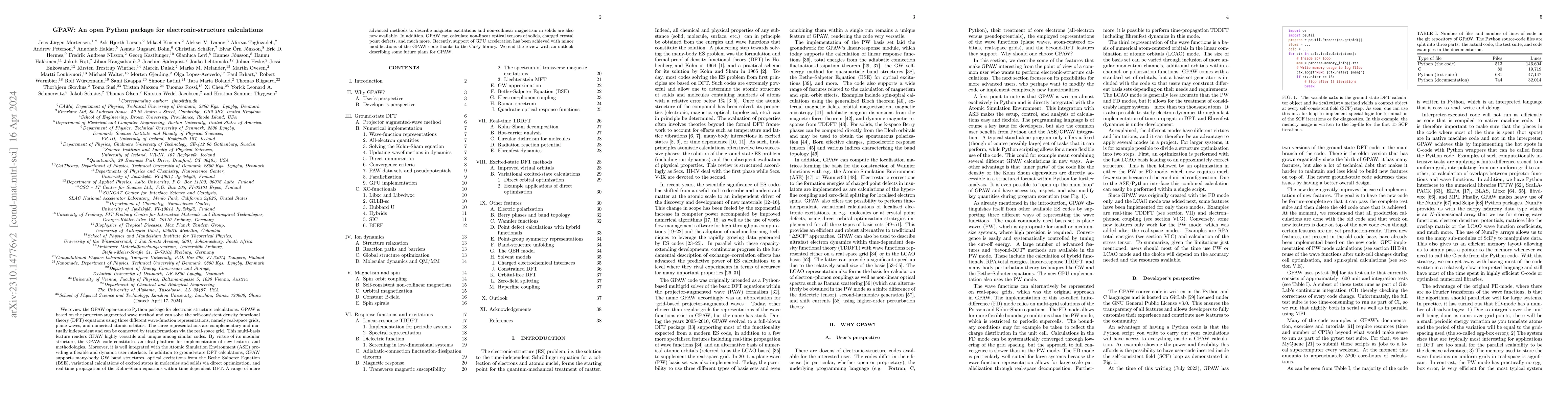
We review the GPAW open-source Python package for electronic structure calculations. GPAW is based on the projector-augmented wave method and can solve the self-consistent density functional theory ...
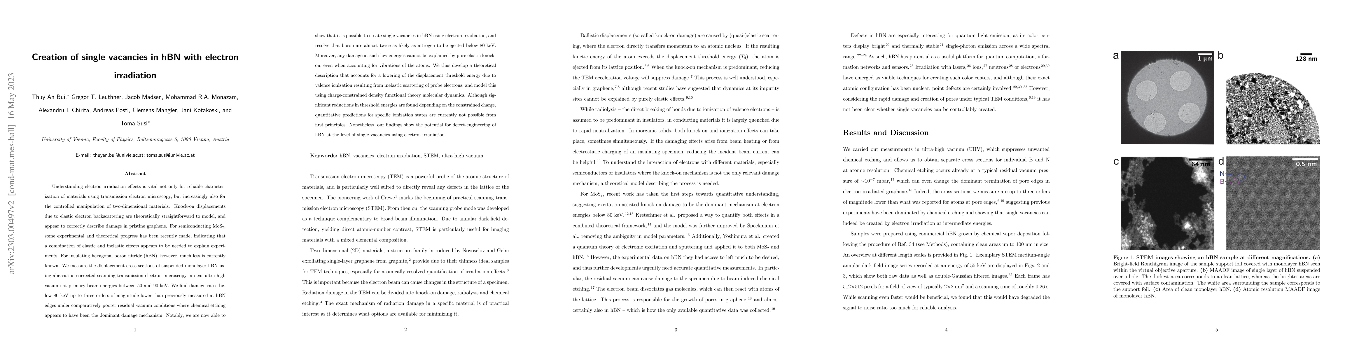
Understanding electron irradiation effects is vital not only for reliable transmission electron microscopy characterization, but increasingly also for the controlled manipulation of two-dimensional ...
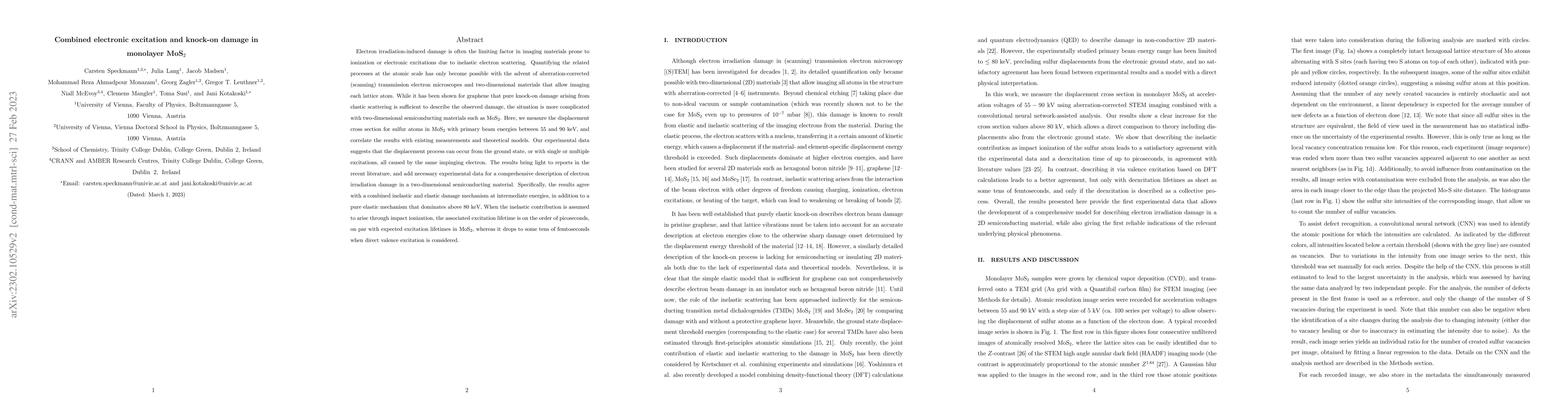
Electron irradiation-induced damage is often the limiting factor in imaging materials prone to ionization or electronic excitations due to inelastic electron scattering. Quantifying the related proc...
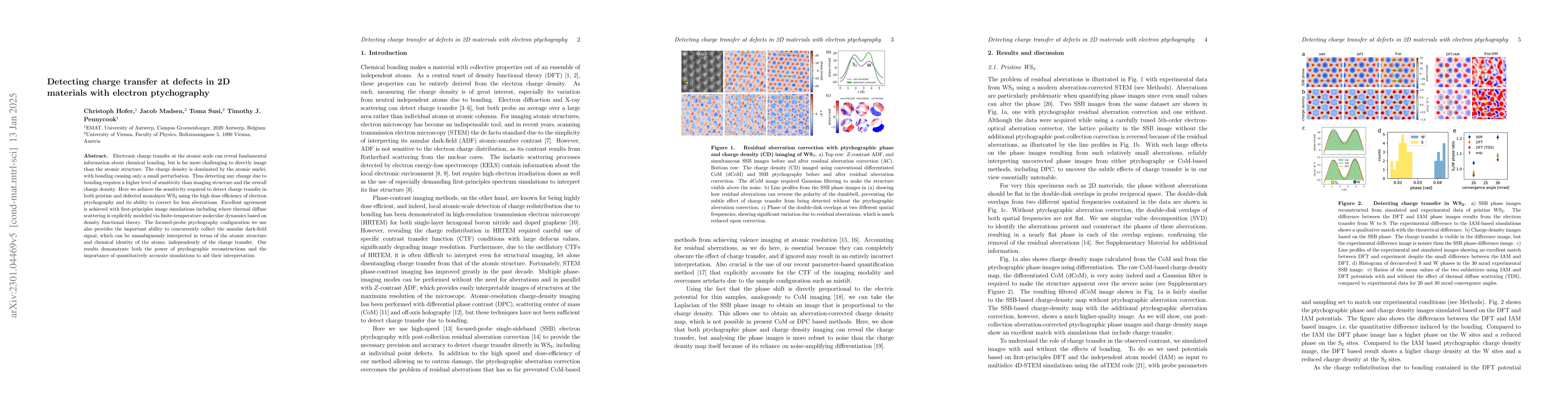
Charge transfer between atoms is fundamental to chemical bonding but has remained very challenging to detect directly in real space. Atomic-resolution imaging of charge density is not sufficient by ...
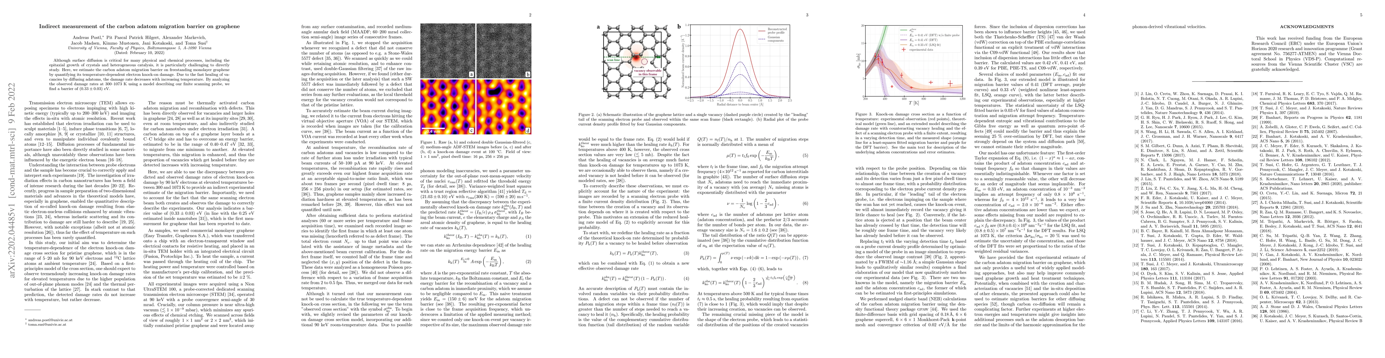
Although surface diffusion is critical for many physical and chemical processes, including the epitaxial growth of crystals and heterogeneous catalysis, it is particularly challenging to directly st...
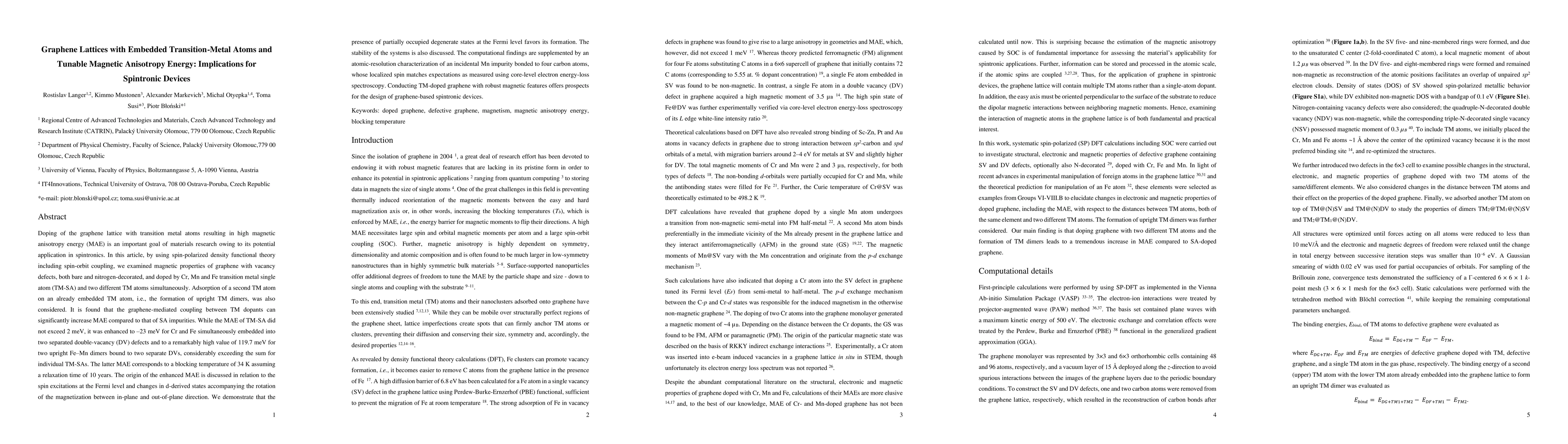
Doping of the graphene lattice with transition metal atoms resulting in high magnetic anisotropy energy (MAE) is an important goal of materials research owing to its potential application in spintro...
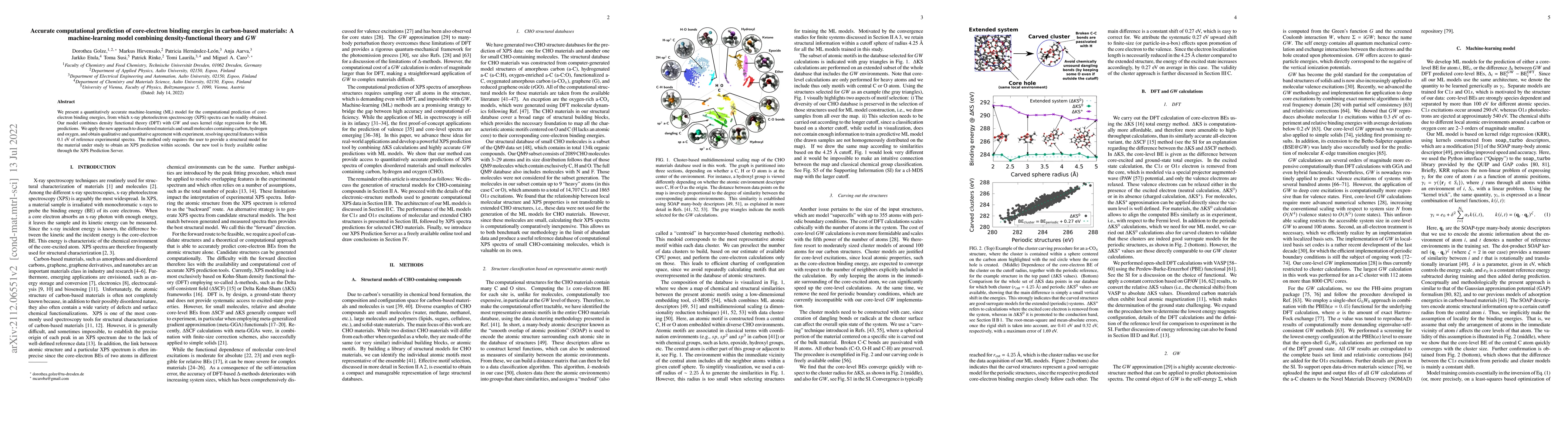
We present a quantitatively accurate machine-learning (ML) model for the computational prediction of core-electron binding energies, from which x-ray photoelectron spectroscopy (XPS) spectra can be ...
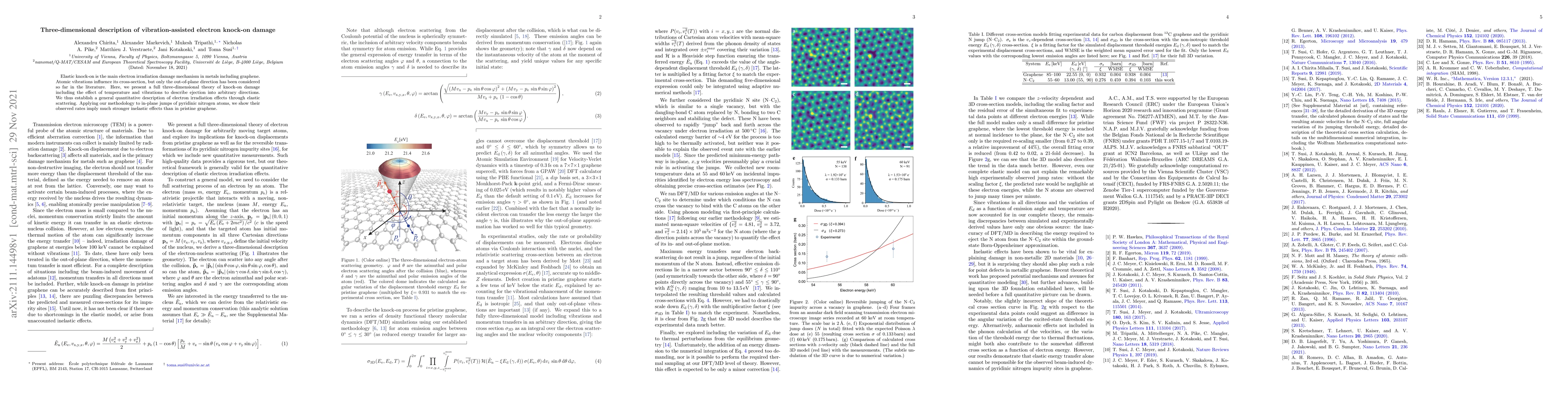
Elastic knock-on is the main electron irradiation damage mechanism in metals including graphene. Atomic vibrations influence its cross-section, but only the out-of-plane direction has been considere...
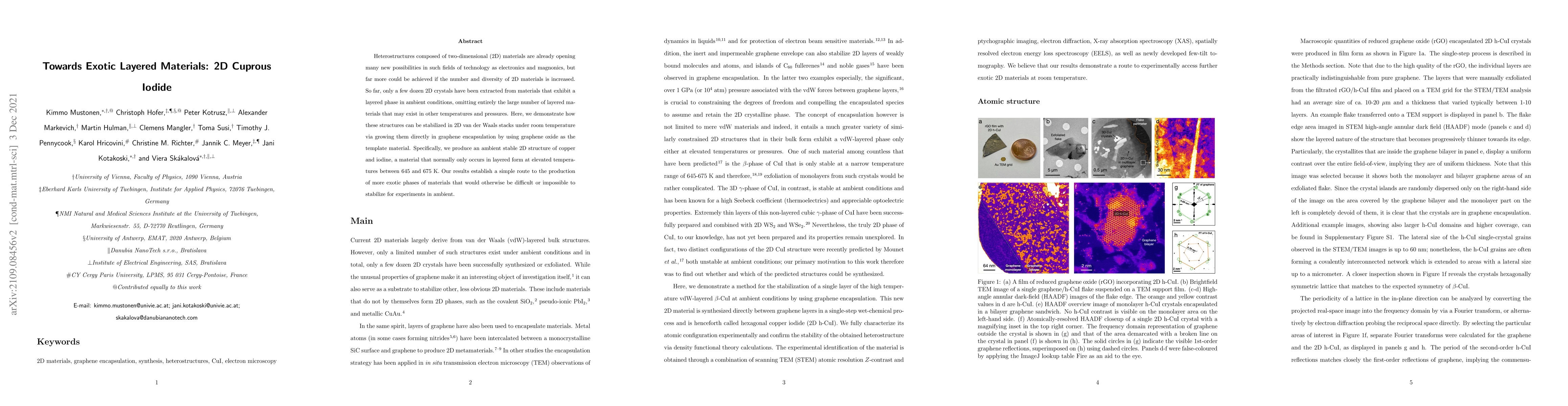
Heterostructures composed of two-dimensional (2D) materials are already opening many new possibilities in such fields of technology as electronics and magnonics, but far more could be achieved if th...
The precise positioning of dopant atoms within bulk crystal lattices could enable novel applications in areas including solid-state sensing and quantum computation. Established scanning probe techni...
Transmission electron microscopy (TEM) and scanning TEM (STEM) are indispensable tools for materials characterization. However, during a typical (S)TEM experiment, the sample is subject to a number ...
Single atoms and few-atom nanoclusters are of high interest in catalysis and plasmonics, but pathways for their fabrication and stable placement remain scarce. We report here the self-assembly of ro...
Important recent advances in transmission electron microscopy instrumentation and capabilities have made it indispensable for atomic-scale materials characterization. At the same time, the availabil...
Porous single layer molybdenum disulfide (MoS$_2$) is a promising material for applications such as DNA sequencing and water desalination. In this work, we introduce irradiation with highly charged ...
The recent discovery that impurity atoms in crystals can be manipulated with focused electron irradiation has opened novel perspectives for top-down atomic engineering. These achievements have been ...
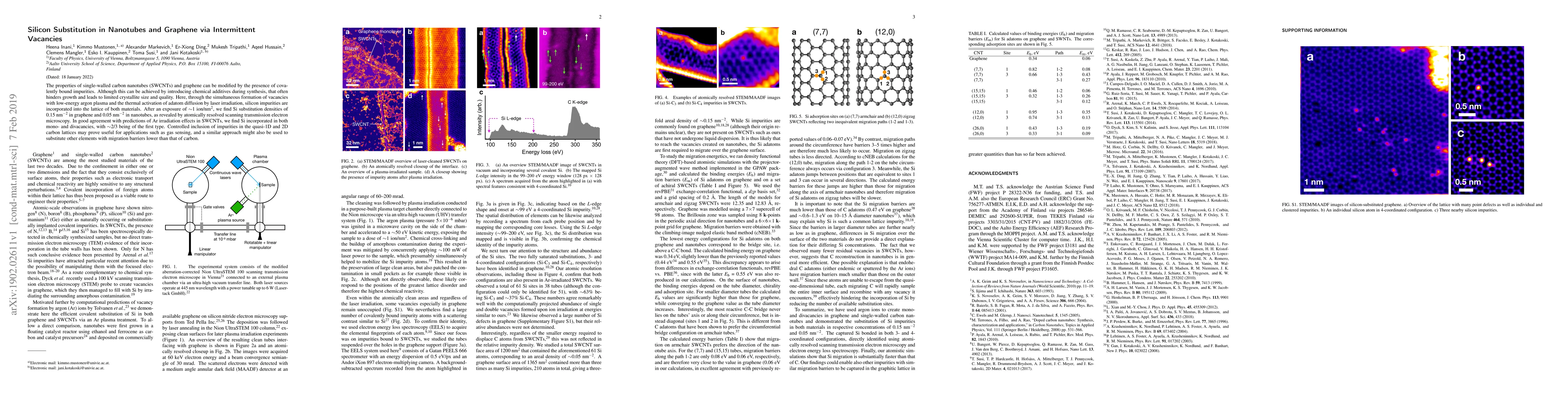
The properties of single-walled carbon nanotubes (SWCNTs) and graphene can be modified by the presence of covalently bound impurities. Although this can be achieved by introducing chemical additives...
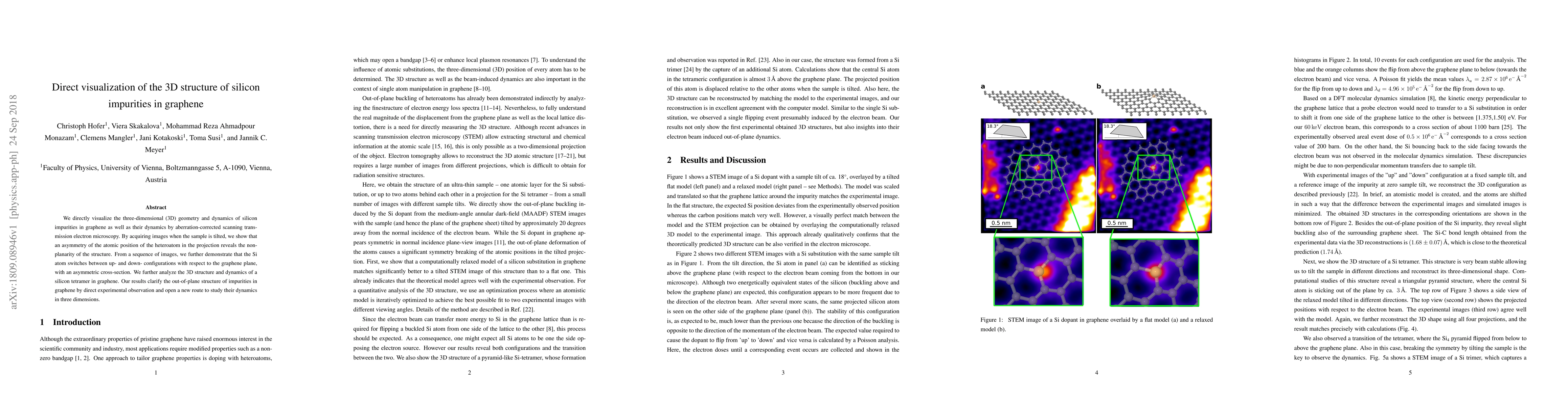
We directly visualize the three-dimensional (3D) geometry and dynamics of silicon impurities in graphene as well as their dynamics by aberration-corrected scanning transmission electron microscopy. ...
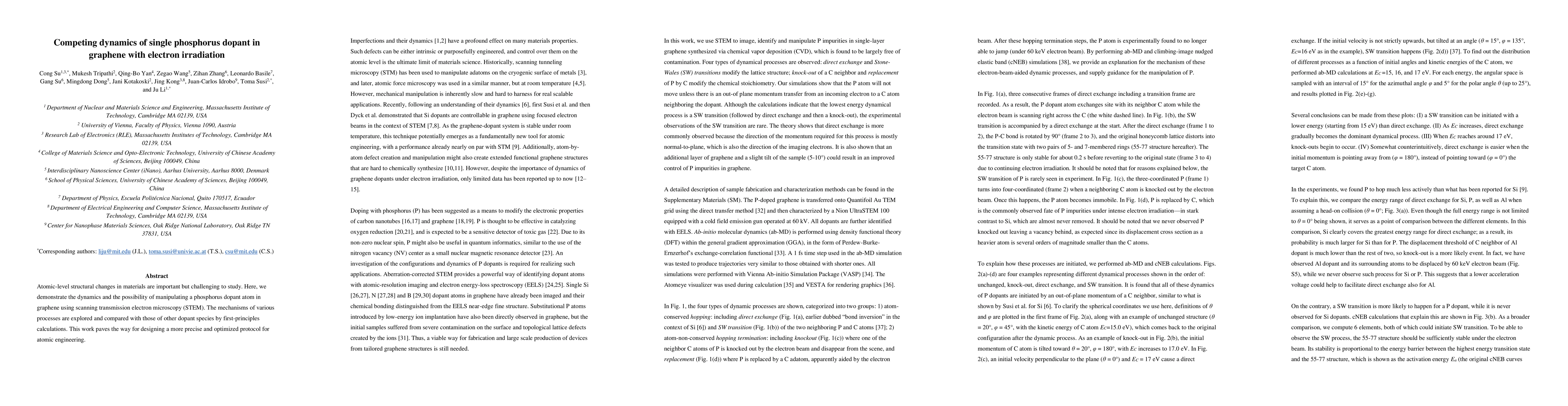
Atomic-level structural changes in materials are important but challenging to study. Here, we demonstrate the dynamics and the possibility of manipulating a phosphorus dopant atom in graphene using ...
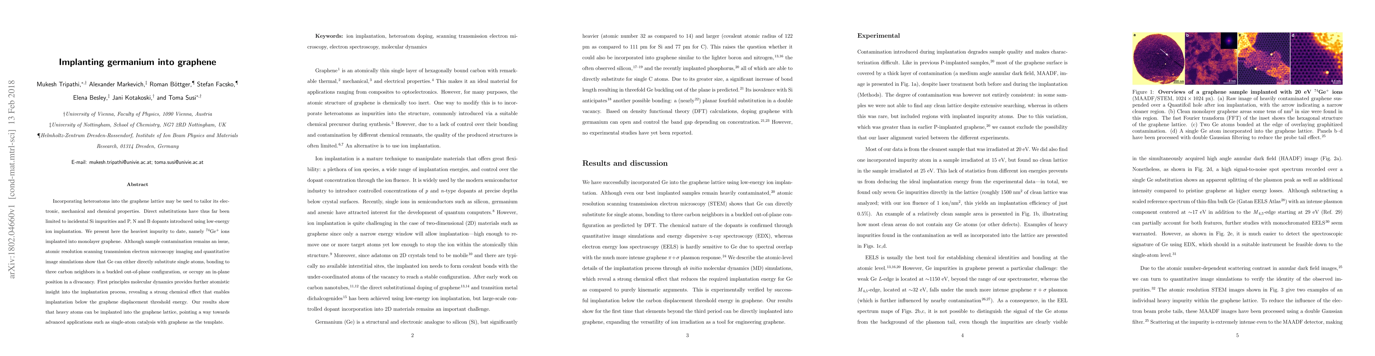
Incorporating heteroatoms into the graphene lattice may be used to tailor its electronic, mechanical and chemical properties. Direct substitutions have thus far been limited to incidental Si impurit...
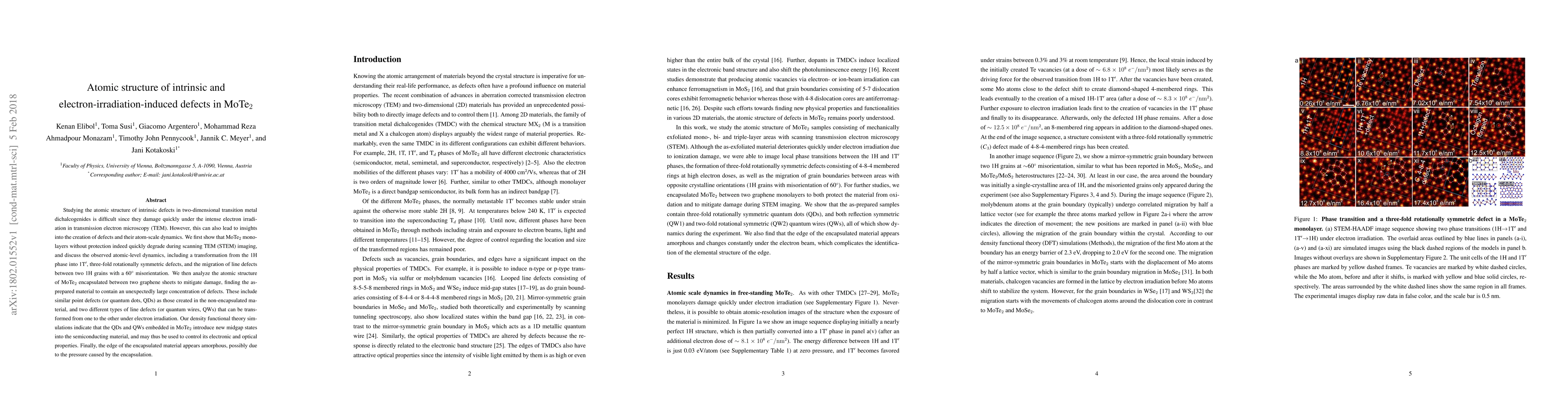
Studying the atomic structure of intrinsic defects in two-dimensional transition metal dichalcogenides is difficult since they damage quickly under the intense electron irradiation in transmission e...
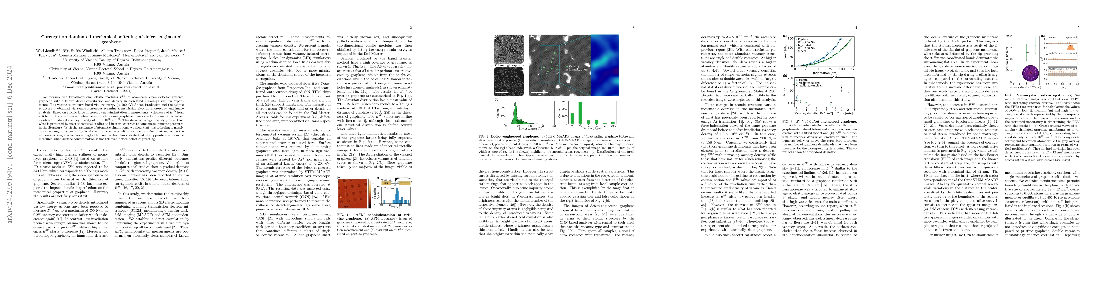
We measure the two-dimensional elastic modulus $E^\text{2D}$ of atomically clean defect-engineered graphene with a known defect distribution and density in correlated ultra-high vacuum experiments. Th...
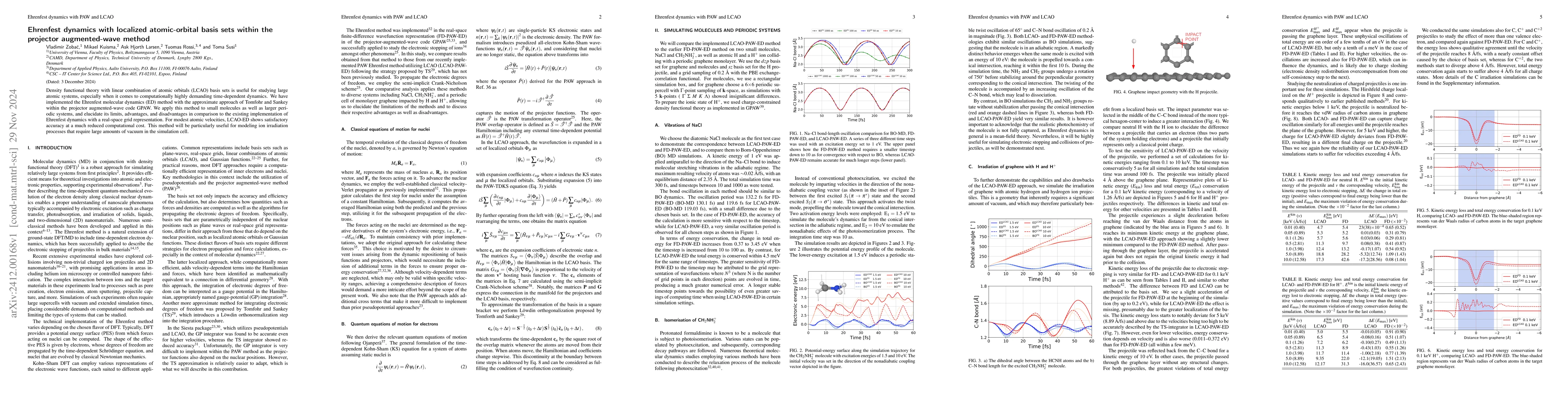
Density functional theory with linear combination of atomic orbitals (LCAO) basis sets is useful for studying large atomic systems, especially when it comes to computationally highly demanding time-de...
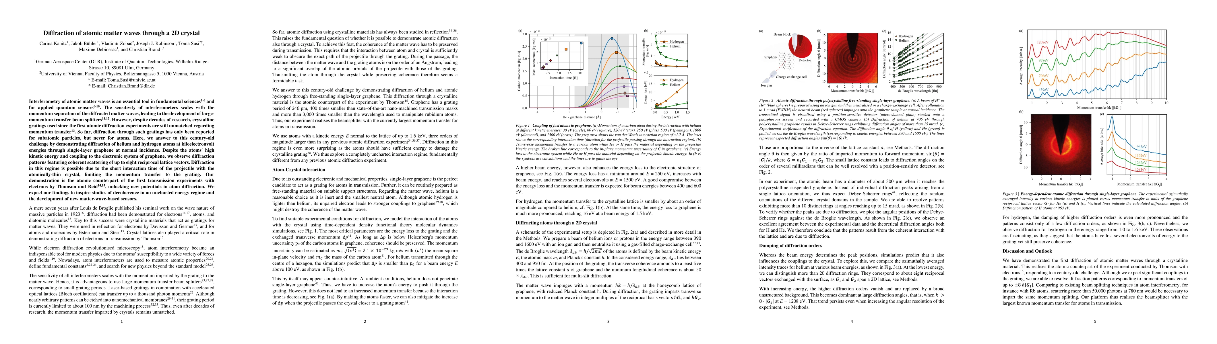
Interferometry of atomic matter waves is an essential tool in fundamental sciences [1-5] and for applied quantum sensors [6-10]. The sensitivity of interferometers scales with the momentum separation ...
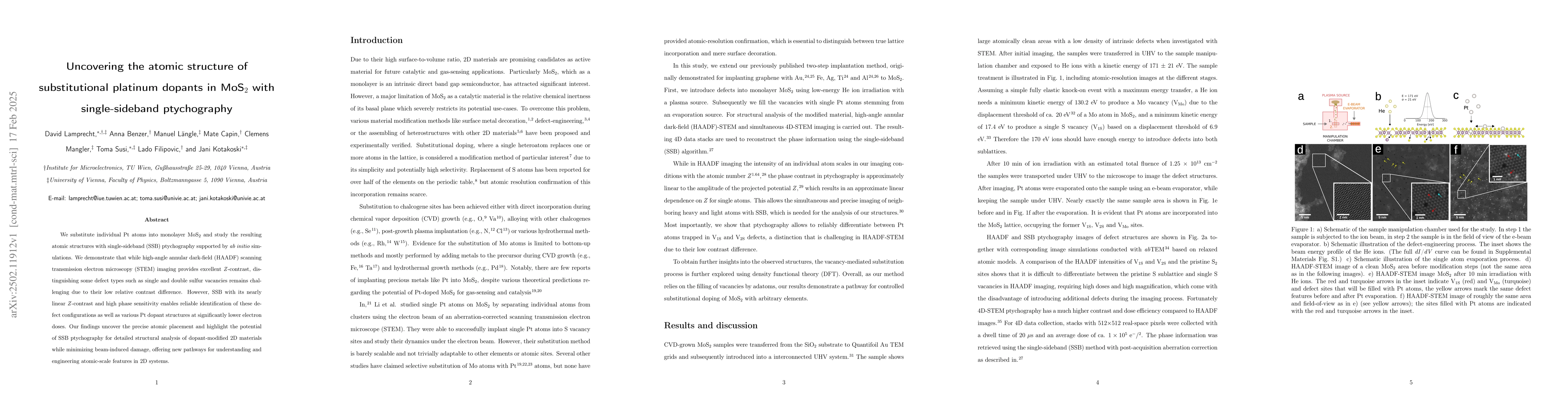
We substitute individual Pt atoms into monolayer MoS$_2$ and study the resulting atomic structures with single-sideband (SSB) ptychography supported by ab initio simulations. We demonstrate that while...
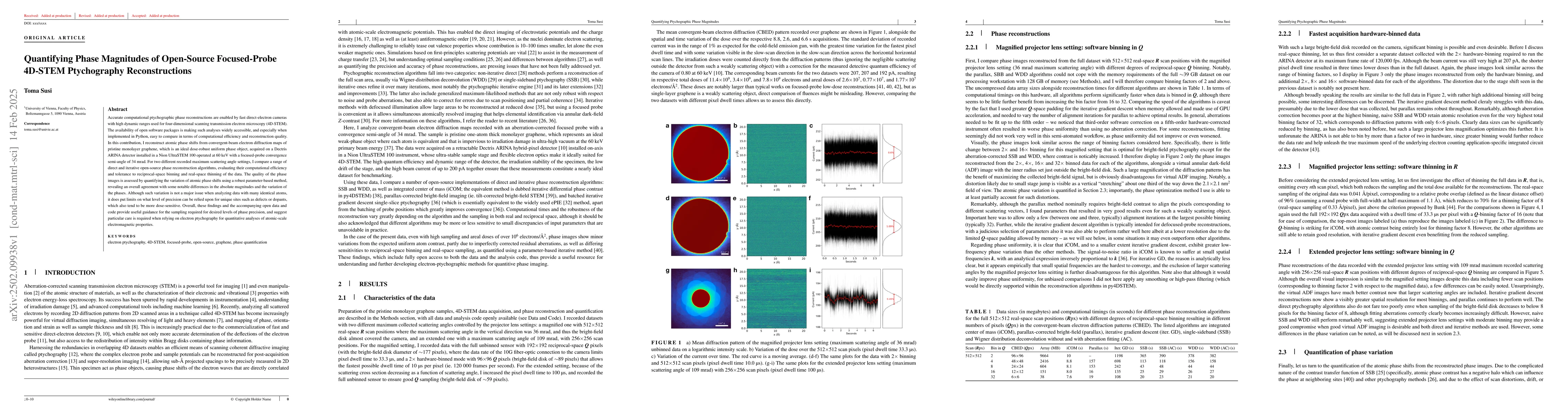
Accurate computational ptychographic phase reconstructions are enabled by fast direct-electron cameras with high dynamic ranges used for four-dimensional scanning transmission electron microscopy (4D-...
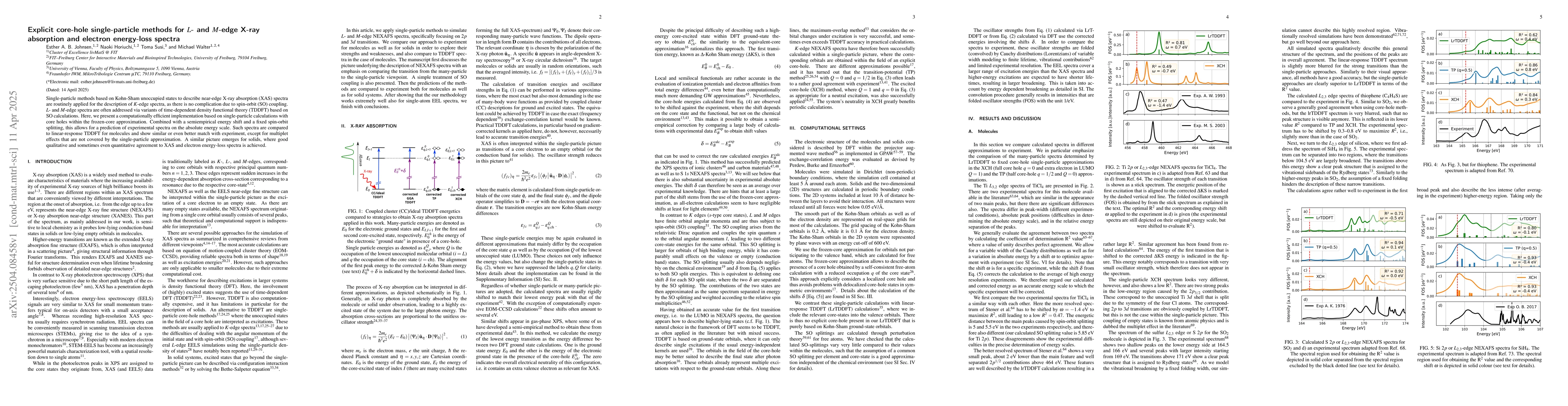
Single-particle methods based on Kohn-Sham unoccupied states to describe near-edge X-ray absorption (XAS) spectra are routinely applied for the description of K-edge spectra, as there is no complicati...
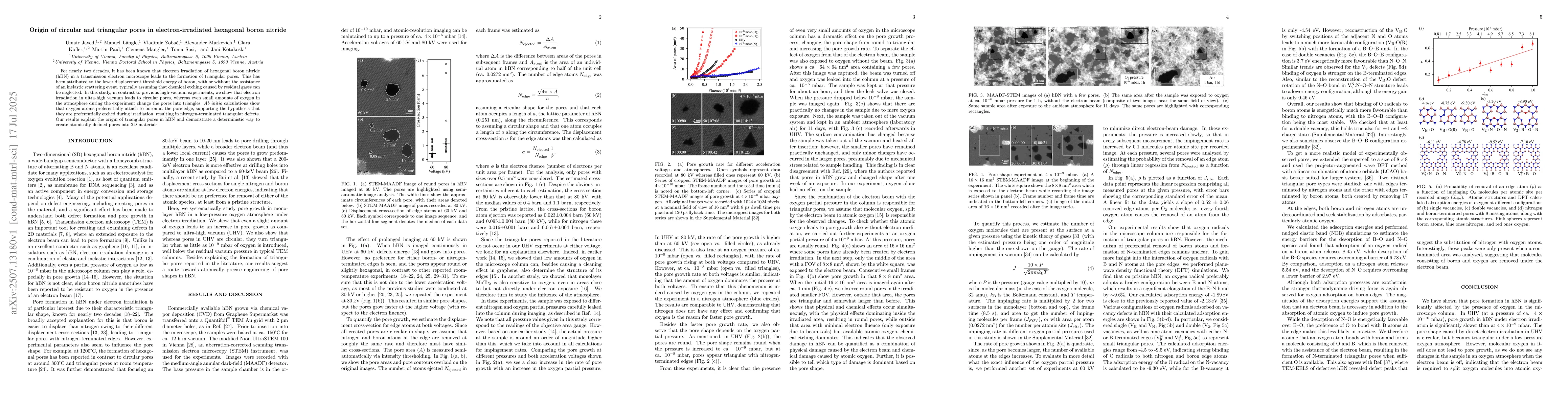
For nearly two decades, it has been known that electron irradiation of hexagonal boron nitride (hBN) in a transmission electron microscope leads to the formation of triangular pores. This has been att...
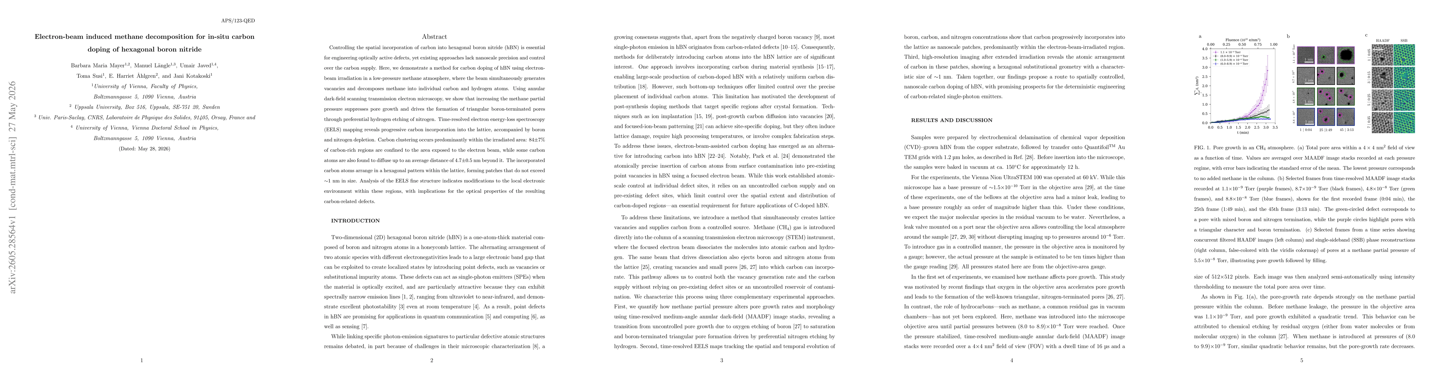
Controlling the spatial incorporation of carbon into hexagonal boron nitride (hBN) is essential for engineering optically active defects, yet existing approaches lack nanoscale precision and control o...
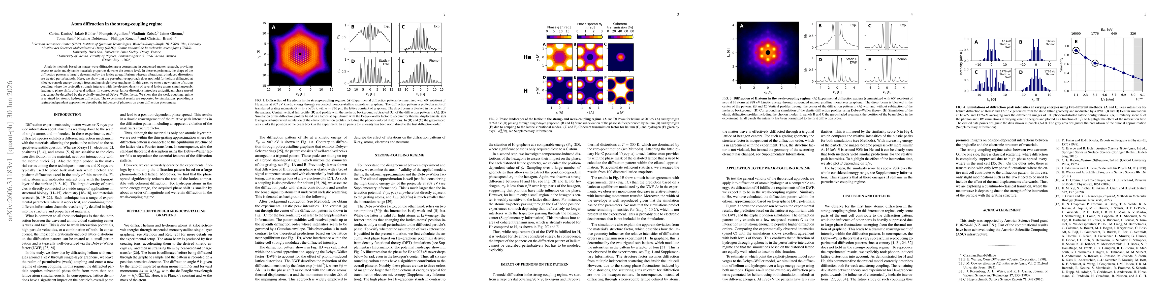
Analytic methods based on matter-wave diffraction are a cornerstone in condensed-matter research, providing access to static and dynamic materials properties down to the atomic level. In these experim...
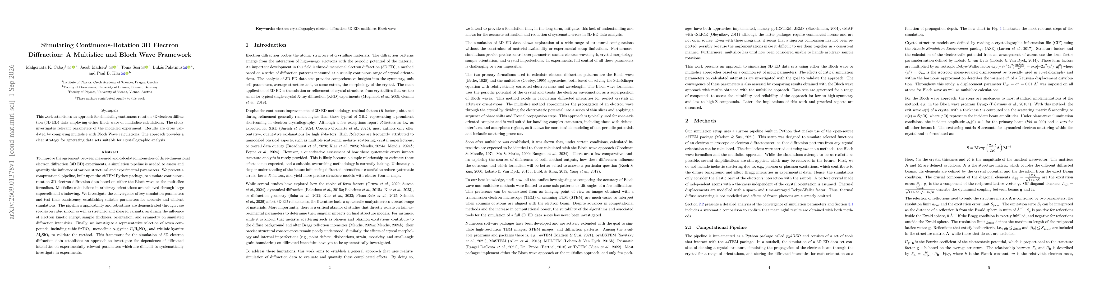
To improve the agreement between measured and calculated intensities of three-dimensional electron diffraction (3D ED) experiments, a simulation pipeline is needed to assess and quantify the influence...
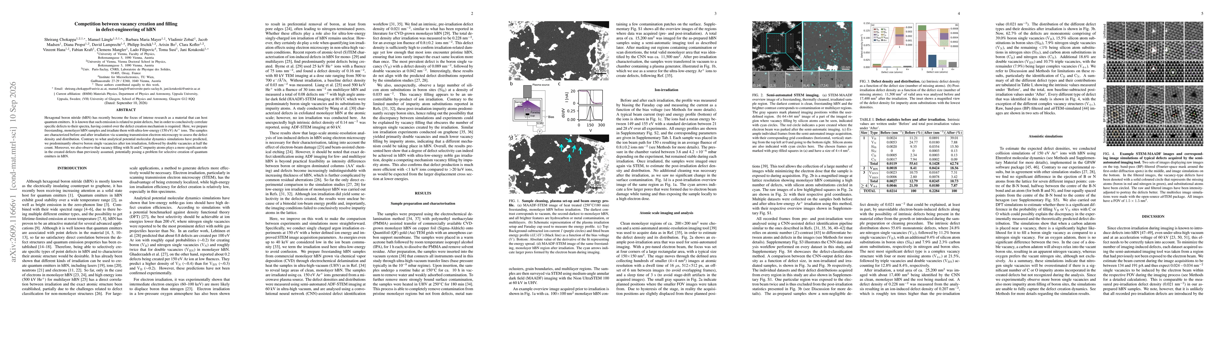
Hexagonal boron nitride (hBN) has recently become the focus of intense research as a material that can host quantum emitters. It is known that such emission is related to point defects, but in order t...