ArxivLens

Publication

Published: Oct 29, 2025
Categories: cond-mat.mtrl-sci, physics.ins-det

Metrics

Source: ArXiv

Quick Answers

What methodology did the authors use?

The study combines four-dimensional scanning transmission electron microscopy (4D-STEM) with electron ptychography to analyze the structural and chiral properties of carbon nanotubes. It uses advanced diffraction techniques to determine chiral indices and detect defects. More in Methodology →

What are the key results?

High-resolution imaging reveals atomic-scale deformations and defects in carbon nanotubes — Chirality engineering techniques enable precise control over nanotube electronic properties More in Key Results →

Why is this work significant?

This research advances nanomaterial characterization, enabling better design of carbon nanotube-based electronics and optoelectronics with controlled chirality and defect structures. More in Significance →

What are the main limitations?

Requires complex and expensive instrumentation — Limited to specific types of carbon nanotubes and materials More in Limitations →

Paper Preview

Abstract

Single wall carbon nanotubes (SWCNT) exhibit remarkable optical and electrical properties making them one of the most promising materials for next generation electronic and optoelectronic devices. Their electronic properties strongly depend on their chirality, i.e., their structural configuration, as well as on the presence and nature of atomic defects. Currently, the lack of versatile and efficient structural characterization techniques limits SWCNT applications. Here, we report how four-dimensional scanning transmission electron microscopy (4D-STEM) can address critical challenges in SWCNT structural analysis. Using modern fast pixelated electron detectors, we were able to acquire rapidly a large number of low noise electron diffraction patterns of SWCNTs. The resulting 4D-STEM data allow to precisely determine the local chirality of multiple nanotubes at once, with limited electron dose (down to 1750 e-/{\AA}^2) and nanometric spatial resolution (down to 3.1 nm). We also show how this approach enables to track the chirality along a single nanotube, while giving access to the strain distribution. Then, we report how 4D-STEM data enable to reconstruct high-resolution images with electron ptychography. With this second approach, structural information can be obtained with atomic scale spatial resolution allowing atomic defect imaging. Finally, we investigate how multi-slice electron ptychography could provide even further insight on nanotube defect structures thanks to its close to 3D imaging capabilities at atomic resolution.
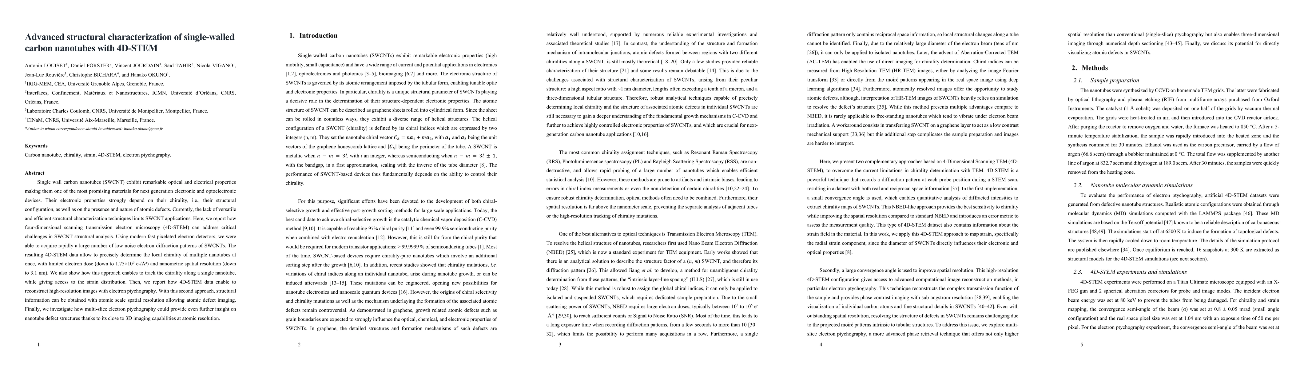
Key Findings, in focus

Seven facets of this paper, analysed and brought into focus by AI.

AI-generated · verify against source Generated Nov 08, 2025
In focus · one-line synthesis

This research advances nanomaterial characterization, enabling better design of carbon nanotube-based electronics and optoelectronics with controlled chirality and defect structures.

01
MethodologyHow they did it

The study combines four-dimensional scanning transmission electron microscopy (4D-STEM) with electron ptychography to analyze the structural and chiral properties of carbon nanotubes. It uses advanced diffraction techniques to determine chiral indices and detect defects.

02
ResultsWhat they found
  • High-resolution imaging reveals atomic-scale deformations and defects in carbon nanotubes
  • Chirality engineering techniques enable precise control over nanotube electronic properties
  • 4D-STEM and ptychography provide unprecedented detail on nanotube structure and defects
03
SignificanceWhy it matters

This research advances nanomaterial characterization, enabling better design of carbon nanotube-based electronics and optoelectronics with controlled chirality and defect structures.

04
Technical ContributionsWhat's new technically

Demonstration of 4D-STEM and ptychography for precise chiral index determination and defect analysis in carbon nanotubes

05
NoveltyWhat sets it apart

First comprehensive application of 4D-STEM and ptychography for both structural analysis and chirality determination in carbon nanotubes

06
LimitationsWhat to be cautious about
  • Requires complex and expensive instrumentation
  • Limited to specific types of carbon nanotubes and materials
07
Future WorkWhere it goes next
  • Development of more accessible 4D-STEM systems
  • Integration with machine learning for automated defect analysis
  • Exploration of defect engineering for novel nanoelectronic applications

Paper Details

Paper ID: 2510.25286
Comments: 41 pages, 12 figures
Categories:
cond-mat.mtrl-sci physics.ins-det

How to Cite This Paper

Reference manager: RIS EndNote


Discussion 0

This website uses cookies to ensure you get the best experience. Learn more