High-Performance Logic and Memory Devices Based on a Dual-Gated MoS2 Architecture
Publication
Metrics
Paper Preview
Abstract
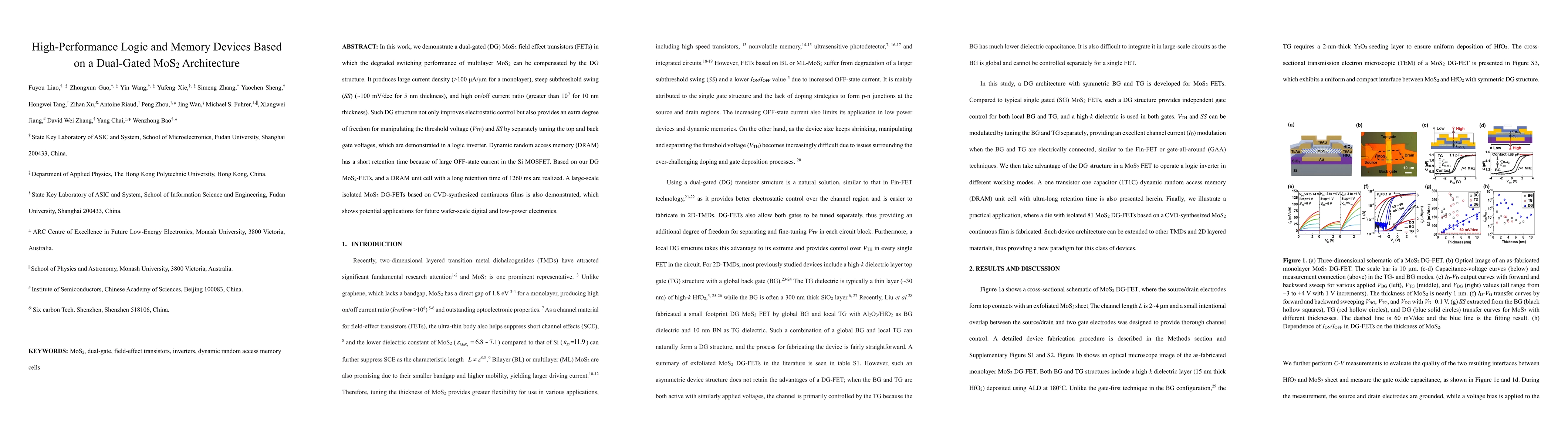
In this work, we demonstrate a dual-gated (DG) MoS2 field effect transistors (FETs) in which the degraded switching performance of multilayer MoS2 can be compensated by the DG structure. It produces large current density (>100 {\mu}A/{\mu}m for a monolayer), steep subthreshold swing (SS) (~100 mV/dec for 5 nm thickness), and high on/off current ratio (greater than 107 for 10 nm thickness). Such DG structure not only improves electrostatic control but also provides an extra degree of freedom for manipulating the threshold voltage (VTH) and SS by separately tuning the top and back gate voltages, which are demonstrated in a logic inverter. Dynamic random access memory (DRAM) has a short retention time because of large OFF-state current in the Si MOSFET. Based on our DG MoS2-FETs, and a DRAM unit cell with a long retention time of 1260 ms are realized. A large-scale isolated MoS2 DG-FETs based on CVD-synthesized continuous films is also demonstrated, which shows potential applications for future wafer-scale digital and low-power electronics.
AI Key Findings
Get AI-generated insights about this paper's methodology, results, significance, and more — seven facets brought into focus.
Impact
Paper Details
Authors
PDF Preview
Key Terms
Citation Network
Current paper (gray), citations (green), references (blue)
Display is limited for performance on very large graphs.
Discussion 0