Publication
Metrics
AI Quick Summary
This research introduces a simple and scalable method to create back gates in high-mobility 2D electron systems using oxygen ion implantation into GaAs layers, which effectively controls conductance without harming surface quality. The technique is compatible with advanced material growth processes and can be applied across entire wafers.
Paper Preview
Abstract
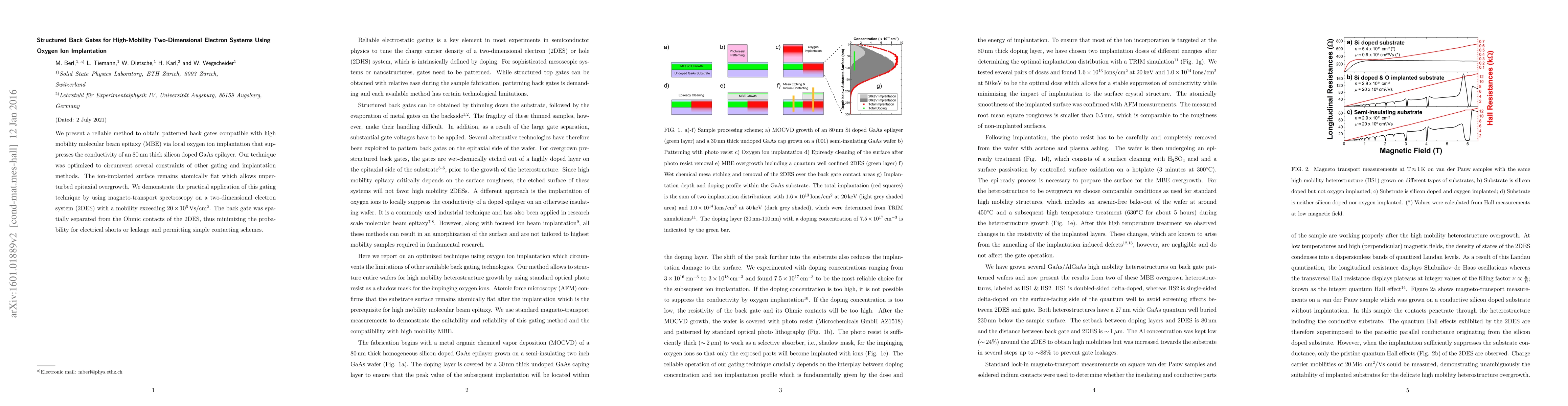
We present a new approach of back gate patterning that is compatible with the requirements of highest mobility molecular beam epitaxy. Contrary to common back gating techniques, our method is simple, reliable and can be scaled up for entire wafers. The back gate structures are defined by local oxygen implantation into a silicon doped GaAs epilayer, which suppresses the conductance without affecting the surface quality.
AI Key Findings
Get AI-generated insights about this paper's methodology, results, significance, and more — seven facets brought into focus.
Impact
Paper Details
PDF Preview
Key Terms
Citation Network
Current paper (gray), citations (green), references (blue)
Display is limited for performance on very large graphs.
Discussion 0