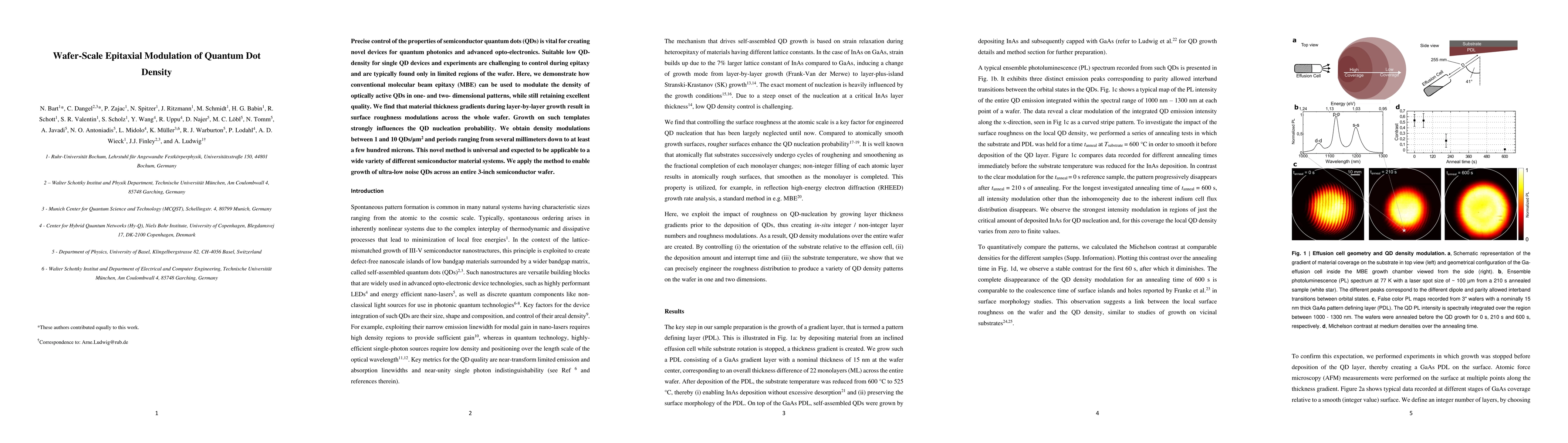
Publication
Metrics
AI Quick Summary
Researchers demonstrate a method to control quantum dot density on wafer scale using molecular beam epitaxy, achieving uniformity across 3-inch wafers with ultra-low noise QDs.
Paper Preview
Abstract
Precise control of the properties of semiconductor quantum dots (QDs) is vital for creating novel devices for quantum photonics and advanced opto-electronics. Suitable low QD-density for single QD devices and experiments are challenging to control during epitaxy and are typically found only in limited regions of the wafer. Here, we demonstrate how conventional molecular beam epitaxy (MBE) can be used to modulate the density of optically active QDs in one- and two- dimensional patterns, while still retaining excellent quality. We find that material thickness gradients during layer-by-layer growth result in surface roughness modulations across the whole wafer. Growth on such templates strongly influences the QD nucleation probability. We obtain density modulations between 1 and 10 QDs/${\mu}m^{2}$ and periods ranging from several millimeters down to at least a few hundred microns. This novel method is universal and expected to be applicable to a wide variety of different semiconductor material systems. We apply the method to enable growth of ultra-low noise QDs across an entire 3-inch semiconductor wafer.
AI Key Findings
Get AI-generated insights about this paper's methodology, results, significance, and more — seven facets brought into focus.
Impact
Paper Details
Authors
PDF Preview
Key Terms
Citation Network
Current paper (gray), citations (green), references (blue)
Display is limited for performance on very large graphs.
Discussion 0