This paper demonstrates that oxygen plasma treatment can significantly improve the performance of MoS2 field effect transistors by mitigating surface defects and contamination, resulting in a substantial reduction in turn-on voltage and increased carrier mobility, while also reducing device-to-device variability.
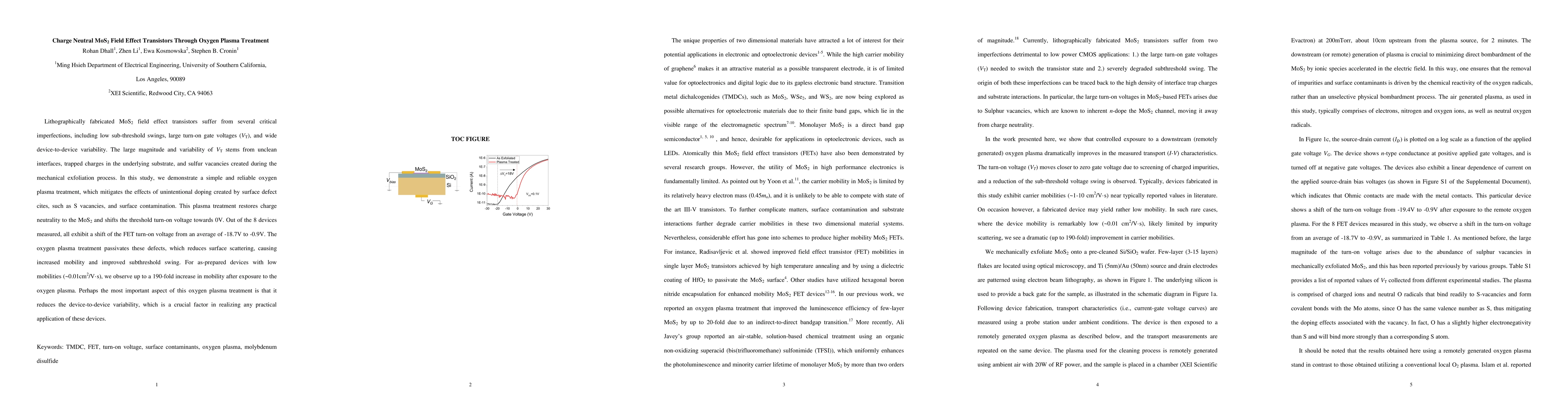
Lithographically fabricated MoS2 field effect transistors suffer from several critical imperfections, including low sub-threshold swings, large turn-on gate voltages (VT), and wide device-to-device variability. The large magnitude and variability of VT stems from unclean interfaces, trapped charges in the underlying substrate, and sulfur vacancies created during the mechanical exfoliation process. In this study, we demonstrate a simple and reliable oxygen plasma treatment, which mitigates the effects of unintentional doping created by surface defect cites, such as S vacancies, and surface contamination. This plasma treatment restores charge neutrality to the MoS2 and shifts the threshold turn-on voltage towards 0V. Out of the 8 devices measured, all exhibit a shift of the FET turn-on voltage from an average of -18.7V to -0.9V. The oxygen plasma treatment passivates these defects, which reduces surface scattering, causing increased mobility and improved subthreshold swing. For as-prepared devices with low mobilities (~0.01cm2/V.s), we observe up to a 190-fold increase in mobility after exposure to the oxygen plasma. Perhaps the most important aspect of this oxygen plasma treatment is that it reduces the device-to-device variability, which is a crucial factor in realizing any practical application of these devices.
This graph shows how this paper is connected to other research. The current paper is shown in dark gray, papers that cite it are in green, and papers it references are in blue. You can:
• Hover over any node to see the paper title
• Click a node to view that paper's details
• Drag nodes to rearrange the graph
• Use the zoom controls (bottom right) to zoom in/out
Title | Authors | Year | Actions |
---|---|---|---|
MoS2 Field-Effect Transistor Performance Enhancement by Contact Doping and Defect Passivation via Fluorine Ions and Its Cyclic Field-Assisted Activation.
|
A. Rai, Asif A. Shah, J. Kumar, Sumana Chattaraj, Aadil Bashir Dar, Utpreksh Patbhaje, M. Shrivastava
|
2024
|
View Paper |
Enabling Oxidation Protection and Carrier-Type Switching for Bismuth Telluride Nanoribbons via in Situ Organic Molecule Coating
|
Jun Beom Park, Wei Wu, Jason Yingzhi Wu, R. Karkee, T. M. Kucinski, K. Bustillo, Matthew M Schneider, David A. Strubbe, Colin Ophus, M. Pettes
|
2023
|
View Paper |
Plasma Processing and Treatment of 2D Transition Metal Dichalcogenides: Tuning Properties and Defect Engineering
|
Saeed Sovizi, Shayan Angizi, Sayed Ali Ahmad Alem, Reyhaneh Goodarzi, Mohammad Reza Rahmani Taji Boyuk, H. Ghanbari, R. Szoszkiewicz, A. Simchi, P. Kruse
|
2023
|
View Paper |
Identification of Ubiquitously Present Polymeric Adlayers on 2D Transition Metal Dichalcogenides
|
Rita Tilmann, C. Bartlam, Oliver Hartwig, Bartłomiej Tywoniuk, Nikolas Dominik, Conor P. Cullen, Lisanne Peters, T. Stimpel‐Lindner, N. McEvoy, G. Duesberg
|
2023
|
View Paper |
A critical review of fabrication challenges and reliability issues in top/bottom gated MoS2 field-effect transistors
|
L. R. Thoutam, R. Mathew, J. Ajayan, Shubham Tayal, S. Nair
|
2023
|
View Paper |
A photon-controlled diode with a new signal-processing behavior
|
Shun Feng, Ruyue Han, Lili Zhang, Chi Liu, Bo Li, Honglei Zhu, Qianbing Zhu, Wei Chen, Hui‐Ming Cheng, Dongming Sun
|
2022
|
View Paper |
Plasma Treatment of Ultrathin Layered Semiconductors for Electronic Device Applications
|
Jakub Jadwiszczak, D. Kelly, Junqing Guo, Yangbo Zhou, Hongzhou Zhang
|
2021
|
View Paper |
Effect of localized helium ion irradiation on the performance of synthetic monolayer MoS2 field-effect transistors
|
Jakub Jadwiszczak, P. Maguire, Conor P. Cullen, G. Duesberg, Hongzhou Zhang
|
2020
|
View Paper |
Formation of Brightly Luminescent MoS2 Nanoislands from Multilayer Flakes via Plasma Treatment and Laser Exposure
|
Bo Wang, Sisi Yang, Y. Wang, Younghee Kim, H. Htoon, S. Doorn, B. Foran, Adam W. Bushmaker, D. Baker, G. Forcherio, S. Cronin
|
2020
|
View Paper |
Large-Scale Atomically Thin Monolayer 2H-MoS2 Field-Effect Transistors
|
N. Shinde, B. Ryu, K. Meganathan, Bellarmine Francis, C. Hong, S. Chandramohan, S. Eswaran
|
2020
|
View Paper |
Measuring Local Electric Fields and Local Charge Densities at Electrode Surfaces using Graphene-enhanced Raman Spectroscopy (GERS)-based Stark-shifts.
|
Haotian Shi, Bofan Zhao, Jie Ma, Mark J. Bronson Jr, Zhi Cai, Jihan Chen, Y. Wang, M. Cronin, L. Jensen, S. Cronin
|
2019
|
View Paper |
Electronic properties of WS2 and WSe2 monolayers with biaxial strain: A first-principles study
|
Do Muoi, N. Hieu, H. Phung, H. Phuc, B. Amin, B. D. Hoi, Nguyen V. Hieu, L. Nhan, C. Nguyen, P. Le
|
2019
|
View Paper |
Direct Patterning of p-Type-Doped Few-layer WSe2 Nanoelectronic Devices by Oxidation Scanning Probe Lithography.
|
A. I. Dago, Y. Ryu, F. Javier Palomares, Ricardo Garcia
|
2018
|
View Paper |
Enhanced thermoelectric efficiency in topological insulator Bi2Te3 nanoplates via atomic layer deposition-based surface passivation
|
Jihan Chen, Jaehyun Kim, Nirakar Poudel, Bingya Hou, L. Shen, Haotian Shi, Li Shi, S. Cronin
|
2018
|
View Paper |
Considerations for Utilizing Sodium Chloride in Epitaxial Molybdenum Disulfide.
|
Kehao Zhang, Brian M. Bersch, Fu Zhang, Natalie C Briggs, S. Subramanian, Ke Xu, M. Chubarov, Ke Wang, J. Lerach, J. Redwing, Susan K. Fullerton‐Shirey, M. Terrones, J. Robinson
|
2018
|
View Paper |
Quantitative analysis of trap states through the behavior of the sulfur ions in MoS2 FETs following high vacuum annealing
|
H. Bae, Sungwoo Jun, C. Kim, B. Ju, Yang‐Kyu Choi
|
2018
|
View Paper |
Radiation-induced direct bandgap transition in few-layer MoS2
|
Bo Wang, Sisi Yang, Jihan Chen, C. Mann, Adam W. Bushmaker, S. Cronin
|
2017
|
View Paper |
Effects of Proton Radiation-Induced Defects on Optoelectronic Properties of MoS2
|
B. Foran, C. Mann, M. Peterson, Adam W. Bushmaker, Bo Wang, Jihan Chen, Sisi Yang, S. Cronin
|
2019
|
View Paper |
Effects of Proton Radiation-Induced Defects on Optoelectronic Properties of MoS<sub>2</sub>
|
B. Foran, C. Mann, M. Peterson, Adam W. Bushmaker, Bo Wang, Jihan Chen, Sisi Yang, S. Cronin
|
2019
|
View Paper |
Published: 2015-06-17
Published: 2015-06-12
Published: 2018-06-06
Comments (0)