ArxivLens

Quick Summary:

This paper presents a method for bidirectional tuning of the threshold voltage in MoS2 field-effect transistors through surface treatment, specifically by adjusting sulfur vacancy levels. The hydrogen treatment technique effectively shifts the threshold voltage without degrading performance, offering a significant step towards the practical application of MoS2 in electronic circuits.

Journal Reference: Nanoscale, 2015,7, 10823-10831
DOI: 10.1039/C5NR00253B
arXiv Id: 1506.04985
Date Published: 2015-06-17
Date Updated: 2015-06-17

Key Terms (TF-IDF):

defect (0.243)
tuning (0.193)
band (0.176)
band gap (0.153)
degradation (0.150)
surface (0.150)
circuits (0.149)
conduction (0.149)
tune (0.146)
left right (0.144)
effect (0.144)
controlling (0.140)
tuned (0.137)
importantly (0.135)
logic (0.135)
creating (0.133)
fold (0.132)
mobility (0.131)
simply (0.131)
slightly (0.130)
License: http://arxiv.org/licenses/nonexclusive-distrib/1.0/

Summary:

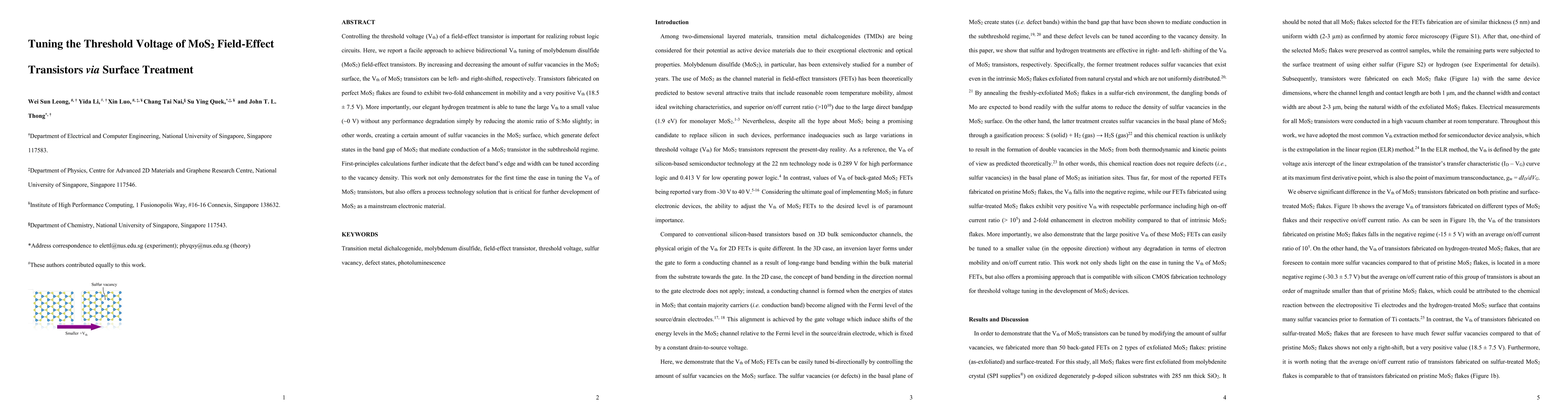
Controlling the threshold voltage (Vth) of a field-effect transistor is important for realizing robust logic circuits. Here, we report a facile approach to achieve bidirectional Vth tuning of molybdenum disulfide (MoS2) field-effect transistors. By increasing and decreasing the amount of sulfur vacancies in the MoS2 surface, the Vth of MoS2 transistors can be left- and right-shifted, respectively. Transistors fabricated on perfect MoS2 flakes are found to exhibit two-fold enhancement in mobility and a very positive Vth. More importantly, our elegant hydrogen treatment is able to tune the large Vth to a small value without any performance degradation simply by reducing the atomic ratio of S:Mo slightly; in other words, creating a certain amount of sulfur vacancies in the MoS2 surface, which generate defect states in the band gap of MoS2 that mediate conduction of a MoS2 transistor in the subthreshold regime. First-principles calculations further indicate that the edge and width of defect band can be tuned according to the vacancy density. This work not only demonstrates for the first time the ease in tuning the Vth of MoS2 transistors, but also offers a process technology solution that is critical for further development of MoS2 as a mainstream electronic material.

Citation & Reference Network Visualization

This graph shows how this paper is connected to other research. The current paper is shown in dark gray, papers that cite it are in green, and papers it references are in blue. You can:

Current Paper
Papers citing this work (Citations)
Papers cited by this work (References)

• Hover over any node to see the paper title

• Click a node to view that paper's details

• Drag nodes to rearrange the graph

• Use the zoom controls (bottom right) to zoom in/out

Citations and References

Title Authors Year Actions
Design of stimuli-responsive transition metal dichalcogenides
R. Torres-Cavanillas, Alicia Forment-Aliaga
2024
View Paper
Bilayer 3R-Stacked MoS2 dual-gate transistor
Renji Bian, Qing Liu, Fucai Liu
2023
View Paper
Effects of forming gas annealing on the doping of monolayer MoS2 crystals
Youjin Koo, Woong Choi
2023
View Paper
Environmentally sustainable implementations of two-dimensional nanomaterials
Mehnaz Shams, Nikhita D. Mansukhani, M. Hersam, D. Bouchard, I. Chowdhury
2023
View Paper
Decreased n-type behavior of monolayer MoS2 crystals annealed in sulfur atmosphere
S. Baik, Youjin Koo, Woong Choi
2022
View Paper
Electron irradiation-induced defects for reliability improvement in monolayer MoS2-based conductive-point memory devices
Xiaohan Wu, Yuqian Gu, Ruijing Ge, Martha I. Serna, Yifu Huang, Jack C. Lee, D. Akinwande
2022
View Paper
Stacking monolayers at will: A scalable device optimization strategy for two-dimensional semiconductors
Xiaojiao Guo, Honglei Chen, J. Bian, Fuyou Liao, Jingyi Ma, Simeng Zhang, Xinzhi Zhang, Junqiang Zhu, C. Luo, Zijian Zhang, Lingyi Zong, Yingdong Xia, Chuming Sheng, Zihan Xu, Saifei Gou, Xinyu Wang, Peng Gong, Liwei Liu, Xixi Jiang, Z. An, C. Cong, Z. Qiu, Xing Wu, P. Zhou, Xinyu Chen, L. Tong, W. Bao
2022
View Paper
Hydrogen Evolution Reaction Catalyst with High Catalytic Activity by Interplay Between Organic Molecules and Transition Metal Dichalcogenide Monolayers
Laud Anim Adofo, Hyung-Jin Kim, F. Agyapong-Fordjour, Huong Thi Thanh Nguyen, Jeong Won Jin, Yong In Kim, Seon Je Kim, Jung Ho Kim, Stephen Boandoh, Soo Ho Choi, Su Jin Lee, S. Yun, Young-Min Kim, S. Kim, Young‐Kyu Han, Ki Kang Kim
2022
View Paper
Healing of donor defect states in monolayer molybdenum disulfide using oxygen-incorporated chemical vapour deposition
Pin-Chun Shen, Y. Lin, C. Su, C. McGahan, Ang-Yu Lu, X. Ji, Xingzhi Wang, Haozhe Wang, Nannan Mao, Yunfan Guo, Ji-Hoon Park, Yan Wang, W. Tisdale, Ju Li, X. Ling, K. Aidala, T. Palacios, Jing Kong
2021
View Paper
On the Contact Optimization of ALD-Based MoS2 FETs: Correlation of Processing Conditions and Interface Chemistry with Device Electrical Performance
R. Mahlouji, Yue Zhang, M. Verheijen, J. Hofmann, W. Kessels, A. Sagade, A. Bol
2021
View Paper
Progress in light-to-frequency conversion circuits based on low dimensional semiconductors
Seung Gi Seo, Seung Yeob Kim, Jinheon Jeong, S. Jin
2021
View Paper
Reversible and controllable threshold voltage modulation for n-channel MoS2 and p-channel MoTe2 field-effect transistors via multiple counter doping with ODTS/poly-L-lysine charge enhancers
Seung Gi Seo, Jinheon Jeong, Seung Yeob Kim, Ajit Kumar, S. Jin
2021
View Paper
Surface functionalization toward top-gated monolayer MoS2 field-effect transistors with ZrO2/Al2O3 as composite dielectrics
T. Guo, Hao Wu, Xi Su, Quanbing Guo, Chang Liu
2021
View Paper
Theoretical analysis of thermal boundary conductance of MoS2-SiO2 and WS2-SiO2 interface
Z. Ong, Yongqing Cai, Gang Zhang, Yong‐Wei Zhang
2020
View Paper
Impact of thermal annealing in forming gas on the optical and electrical properties of MoS2 monolayer
F. Iacovella, A. Koroleva, A. Rybkin, M. Fouskaki, N. Chaniotakis, P. Savvidis, G. Deligeorgis
2020
View Paper
Enhancement of photodetection by PbSe quantum dots on atomic-layered GeS devices
Yuzhi Li, Xuan Shi, Fangbo Dai, Dahua Zhou, Ming-xing Jin, Hongying Zheng, Yuhui Yang, Hongquan Zhao, Junzhong Wang
2020
View Paper
High-performance flexible nanoscale transistors based on transition metal dichalcogenides
A. Daus, S. Vaziri, Victoria Chen, Ç. Köroğlu, R. Grady, C. Bailey, H. Lee, K. Schauble, K. Brenner, E. Pop
2020
View Paper
A new approach for nano-structuring of glassy selenium (g-Se) using silver nanoparticles (AgNPs) as precursor
Ajay Kumar, N. Mehta, A. Dahshan
2020
View Paper
Changing the Electronic Polarizability of Monolayer MoS2 by Perylene‐Based Seeding Promoters
C. Martella, E. Kozma, Pinakapani Tummala, Saverio Ricci, K. A. Patel, Anita Andicsová‐Eckstein, F. Bertini, G. Scavia, R. Sordan, L. Nobili, M. Bollani, U. Giovanella, A. Lamperti, A. Molle
2020
View Paper
Atomic Layer MoS2xTe2(1-x) Ternary Alloys: Two-Dimensional van der Waals Growth, Bandgap Engineering, and Electrical Transport.
Dong-Ho Kim, Guen Hyung Oh, A. Kim, Chaeho Shin, Jonghoo Park, Sang‐il Kim, Taewan Kim
2020
View Paper
Electrically Tunable Room Temperature Hysteresis Crossover in Underlap MoS$_2$ FETs
Himani Jawa, Abin Varghese, S. Lodha
2020
View Paper
Artificial Intelligence Algorithm Enabled Industrial-Scale Graphene Characterization
W. Leong, G. Arrabito, G. Prestopino
2020
View Paper
Correlation between threshold voltage and its pre-exponential factor in resistive switching
A. Srivastava, S. Pal, N. Mehta
2020
View Paper
Detecting the Repair of Sulfur Vacancies in CVD-Grown MoS2 Domains via Hydrogen Etching
Shike Hu, Jing Li, Shuang Wang, Yijian Liang, He Kang, Yanhui Zhang, Zhiying Chen, Y. Sui, G. Yu, Song-ang Peng, Zhi Jin, Xinyu Liu
2020
View Paper
Optimizing Al-doped ZrO2 as the gate dielectric for MoS2 field-effect transistors
Xingjuan Song, Jingping Xu, Lu Liu, Yu-Heng Deng, Puxiang Lai, Wing-Man Tang
2019
View Paper
Studies of high field conduction and resistive switching in Se78-xTe20Sn2Gex (0 ≤ x ≤ 6) bulk glasses using current-voltage characteristics
S. Pal, A. Srivastava, N. Mehta
2019
View Paper
Physical effects of passivation and creation of sulphur vacancy in MoS2 nanoparticles
R. A. Roshini, E. S. Kannan
2019
View Paper
Engineering Field Effect Transistors with 2D Semiconducting Channels: Status and Prospects
X. Jing, Y. Illarionov, E. Yalon, P. Zhou, T. Grasser, Yuanyuan Shi, M. Lanza
2019
View Paper
Reliability of scalable MoS2 FETs with 2 nm crystalline CaF2 insulators
Y. Illarionov, A. Banshchikov, D. Polyushkin, S. Wachter, T. Knobloch, M. Thesberg, M. Vexler, M. Waltl, M. Lanza, N. Sokolov, T. Mueller, T. Grasser
2019
View Paper
Functionalized MoS2-erlotinib produces hyperthermia under NIR
Chen Zhang, Doudou Zhang, Jian Liu, Jie Wang, Yusheng Lu, Junxia Zheng, Bifei Li, L. Jia
2019
View Paper
Selective Engineering of Chalcogen Defects in MoS2 by Low-Energy Helium Plasma.
Binjie Huang, F. Tian, Youde Shen, Minrui Zheng, Yunshan Zhao, Jing Wu, Yi Liu, S. Pennycook, J. Thong
2019
View Paper
Ultrathin calcium fluoride insulators for two-dimensional field-effect transistors
Y. Illarionov, A. Banshchikov, D. Polyushkin, S. Wachter, T. Knobloch, M. Thesberg, L. Mennel, Matthias Paur, M. Stöger-Pollach, A. Steiger-Thirsfeld, M. Vexler, M. Waltl, N. Sokolov, T. Mueller, T. Grasser
2019
View Paper
Artificial Synapses Based on Multiterminal Memtransistors for Neuromorphic Application
Lin Wang, W. Liao, S. L. Wong, Z. Yu, Sifan Li, Y. Lim, Xuewei Feng, W. Tan, Xin Huang, Li Chen, Liang Liu, Jingsheng Chen, X. Gong, Chunxiang Zhu, Xinke Liu, Yong‐Wei Zhang, D. Chi, K. Ang
2019
View Paper
Threshold Voltage Control of Multilayered MoS2 Field-Effect Transistors via Octadecyltrichlorosilane and their Applications to Active Matrixed Quantum Dot Displays Driven by Enhancement-Mode Logic Gates.
Jeongkyun Roh, Jae Hyeon Ryu, G. Baek, Heeyoung Jung, Seung Gi Seo, Kunsik An, Byeong Guk Jeong, Doh C. Lee, B. Hong, W. Bae, Jong-Ho Lee, Changhee Lee, S. Jin
2019
View Paper
Charge Transfer within the F4TCNQ‐MoS2 van der Waals Interface: Toward Electrical Properties Tuning and Gas Sensing Application
Jiawei Wang, Z. Ji, G. Z. Yang, X. Chuai, Fengjing Liu, Zheng Zhou, Congyan Lu, Wei Wei, Xuewen Shi, J. Niu, Liang Wang, Hong Wang, Jiezhi Chen, Nianduan Lu, Chao Jiang, Ling Li, Ming Liu
2018
View Paper
Experimentally Measured Field Effect Mobilities for Few Layer van der Waals Materials
S. Sylvia, R. Lake
2018
View Paper
CVD Technology for 2-D Materials
Pin-Chun Shen, Y. Lin, Haozhe Wang, Ji-Hoon Park, W. Leong, Ang-Yu Lu, T. Palacios, J. Kong
2018
View Paper
2D MoSe2 Transistor with Polymer‐Brush/Channel Interface
Yeonsu Jeong, Ji Hoon Park, Jongtae Ahn, June Yeong Lim, Eunkyoung Kim, S. Im
2018
View Paper
The organic-2D transition metal dichalcogenide heterointerface.
Y. Huang, Y. Zheng, Zhibo Song, D. Chi, A. Wee, S. Y. Quek
2018
View Paper
Wavelength-selective enhancement of photo-responsivity in metal-gated multi-layer MoS2 phototransistors
Sanghyun Lee, Youngseo Park, G. Yoo, J. Heo
2017
View Paper
Oxide-mediated recovery of field-effect mobility in plasma-treated MoS2
Jakub Jadwiszczak, C. O’Callaghan, Yangbo Zhou, D. Fox, Eamonn Weitz, D. Keane, Conor P. Cullen, I. O'Reilly, C. Downing, A. Shmeliov, P. Maguire, J. J. Gough, C. McGuinness, M. Ferreira, A. L. Bradley, J. Boland, G. Duesberg, V. Nicolosi, Hongzhou Zhang
2017
View Paper
Triethanolamine doped multilayer MoS2 field effect transistors.
Min-Yeul Ryu, H. Jang, K. Lee, Mingxing Piao, S. Ko, M. Shin, J. Huh, Gyu-Tae Kim
2017
View Paper
Green synthesis of luminescent and defect-free bio-nanosheets of MoS2: interfacing two-dimensional crystals with hydrophobins
Jasneet Kaur, A. M. Gravagnuolo, P. Maddalena, C. Altucci, P. Giardina, F. Gesuele
2017
View Paper
Split-gated point-contact for electrostatic confinement of transport in MoS2/h-BN hybrid structures
C. Sharma, M. Thalakulam
2017
View Paper
Spin-dependent thermoelectric effects in Fe-C6 doped monolayer MoS2
Lin Zhu, F. Zou, G. Gao, K. Yao
2017
View Paper
p-Type transition-metal doping of large-area MoS2 thin films grown by chemical vapor deposition.
Enzhi Xu, Haoming Liu, Kyungwha Park, Zhen Li, Yaroslav Losovyj, M. Starr, Madilynn Werbianskyj, H. Fertig, Shixiong Zhang
2017
View Paper
Effects of Growth Conditions on the Measured Electrical Properties of Monolayer Molybdenum Disulfide
A. Mazzoni, R. Burke, M. Chin, Matthew J. Hwee
2017
View Paper
Impact and Origin of Interface States in MOS Capacitor with Monolayer MoS2 and HfO2 High-k Dielectric
P. Xia, Xuewei Feng, Rui Jie Ng, Shijie Wang, D. Chi, Cequn Li, Zhubing He, Xinke Liu, K. Ang
2017
View Paper
Topography preserved microwave plasma etching for top-down layer engineering in MoS2 and other van der Waals materials.
Abin Varghese, C. Sharma, M. Thalakulam
2016
View Paper
Gate dielectric ion implantation to modulate the threshold voltage of In2O3 nanowire field effect transistors
Yang Yu, Wenqing Li, Pengcheng Wu, Changzhong Jiang, Xiangheng Xiao
2016
View Paper
Investigations of vapour-phase deposited transition metal dichalcogenide films for future electronic applications
Riley Gatensby, T. Hallam, Kangho Lee, N. McEvoy, G. Duesberg
2016
View Paper
Two-dimensional van der Waals nanosheet devices for future electronics and photonics
Kyunghee Choi, Young Tack Lee, S. Im
2016
View Paper
Thickness-Dependent Binding Energy Shift in Few-Layer MoS2 Grown by Chemical Vapor Deposition.
Yu-Kai Lin, Ruei-San Chen, Tsu-chin Chou, Yi-Hsin Lee, Y. Chen, Kuei-Hsien Chen, Li‐Chyong Chen
2016
View Paper
Enhancement-mode operation of multilayer MoS2 transistors with a fluoropolymer gate dielectric layer
G. Yoo, Sol Lea Choi, Sue-Yoen Lee, B. Yoo, Sunkook Kim, M. Oh
2016
View Paper
Chemical free device fabrication of two dimensional van der Waals materials based transistors by using one-off stamping
Young Tack Lee, W. Choi, D. Hwang
2016
View Paper
Surface defect passivation of MoS2 by sulfur, selenium, and tellurium
Ying Wang, Long Qi, Lei Shen, Yihong Wu
2016
View Paper
Temperature dependence of the critical points of monolayer MoS2 by ellipsometry
Han Gyeol Park, Tae Jung Kim, Hwa Seob Kim, C. H. Yoo, Nilesh S. Barange, V. L. Le, H. Kim, V. Senthilkumar, C. Le, Yong Soo Kim, M. Seong, Y. D. Kim
2016
View Paper
Ballistic thermal transport in monolayer transition-metal dichalcogenides: Role of atomic mass
Jinlong Ma, Wu Li, Xiaobing Luo
2016
View Paper
Temperature-controlled spin filter and spin valve based on Fe-doped monolayer MoS2.
F. Zou, Lin Zhu, Gaoying Gao, Menghao Wu, K. Yao
2016
View Paper
One-pot synthesis of multidimensional conducting polymer nanotubes for superior performance field-effect transistor-type carcinoembryonic antigen biosensors
Jin Wook Park, Wonjoo Na, J. Jang
2016
View Paper
Nonequilibrium spin injection in monolayer black phosphorus.
Mingyang Chen, Zhizhou Yu, Yin Wang, Yiqun Xie, Jian Wang, Hong Guo
2016
View Paper
Hysteresis-reversible MoS2 transistor
Banglin Cao, Zegao Wang, Xuya Xiong, Ling Gao, Jiheng Li, M. Dong
2021
View Paper
Electrical and Physical Comparison of MoS2 Monolayers Synthesized Via CVD in Different Carrier Gas Environments APPROVED BY SUPERVISING COMMITTEE:
Marie Depoy
2020
View Paper

Comments (0)

This website uses cookies to ensure you get the best experience. Learn more