ArxivLens

Publication

Published: Jul 20, 2026
Categories: cond-mat.mtrl-sci, physics.ins-det, quant-ph

Metrics

Source: ArXiv

Quick Answers

What methodology did the authors use?

The study repurposes a commercial 65-nm CMOS process by functionally partitioning its metal stack into microwave, thermal, and electrical subsystems within a 1 mm2 footprint, enabling integrated RF delivery, cryogenic operation down to 1.75 K, optical access for ODMR, and compatibility with in-situ electron-beam imaging. More in Methodology →

What are the key results?

Demonstrated cryogenic magnetic susceptibility measurements of Fe3GeTe2 heterostructures at 1.75 K without sample-specific fabrication. — Achieved NV-center ODMR with greater than 20% contrast at 4–9 dBm microwave power, reducing required power by 20–25 dB relative to conventional antennas while maintaining 2–3 μT/√Hz sensitivity. More in Key Results →

Why is this work significant?

Provides a scalable, foundry-manufacturable multimodal quantum sensing and materials characterization platform that integrates microwave delivery, electrical/thermal interfacing, and optical access within a compact CMOS footprint, potentially enabling reproducible workflows across laboratories. More in Significance →

What are the main limitations?

Demonstrations are limited to specific modalities (NV ODMR, cryogenic magnetometry, and electron-beam imaging) and may not yet cover all potential quantum materials probes. — Reliance on a particular 65-nm CMOS process may constrain cross-foundry customization and long-term supply stability. More in Limitations →

Paper Preview

Abstract

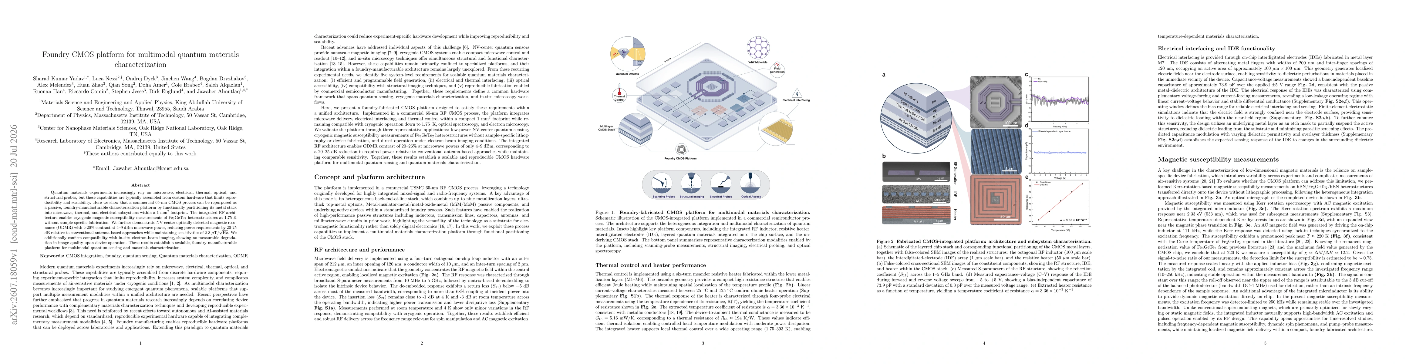
Quantum materials experiments increasingly rely on microwave, electrical, thermal, optical, and structural probes, but these capabilities are typically assembled from custom hardware that limits reproducibility and scalability. Here we show that a commercial 65-nm CMOS process can be repurposed as a passive, foundry-manufacturable characterization platform by functionally partitioning its metal stack into microwave, thermal, and electrical subsystems within a 1 mm2 footprint. The integrated RF architecture enables cryogenic magnetic susceptibility measurements of Fe3GeTe2 heterostructures at 1.75 K without sample-specific fabrication. We further demonstrate NV-center optically detected magnetic resonance (ODMR) with >20% contrast at 4-9 dBm microwave power, reducing power requirements by 20-25 dB relative to conventional antenna-based approaches while maintaining sensitivities of 2-3 uT/sqrt(Hz). We additionally confirm compatibility with in-situ electron-beam imaging, showing no measurable degradation in image quality upon device operation. These results establish a scalable, foundry-manufacturable platform for multimodal quantum sensing and materials characterization.
Key Findings, in focus

Seven facets of this paper, analysed and brought into focus by AI.

AI-generated · verify against source Generated Jul 22, 2026
In focus · one-line synthesis

Provides a scalable, foundry-manufacturable multimodal quantum sensing and materials characterization platform that integrates microwave delivery, electrical/thermal interfacing, and optical access within a compact CMOS footprint, potentially enabling reproducible workflows across laboratories.

01
MethodologyHow they did it

The study repurposes a commercial 65-nm CMOS process by functionally partitioning its metal stack into microwave, thermal, and electrical subsystems within a 1 mm2 footprint, enabling integrated RF delivery, cryogenic operation down to 1.75 K, optical access for ODMR, and compatibility with in-situ electron-beam imaging.

02
ResultsWhat they found
  • Demonstrated cryogenic magnetic susceptibility measurements of Fe3GeTe2 heterostructures at 1.75 K without sample-specific fabrication.
  • Achieved NV-center ODMR with greater than 20% contrast at 4–9 dBm microwave power, reducing required power by 20–25 dB relative to conventional antennas while maintaining 2–3 μT/√Hz sensitivity.
  • Validated compatibility with in-situ electron-beam imaging, showing no measurable degradation in image quality during device operation.
03
SignificanceWhy it matters

Provides a scalable, foundry-manufacturable multimodal quantum sensing and materials characterization platform that integrates microwave delivery, electrical/thermal interfacing, and optical access within a compact CMOS footprint, potentially enabling reproducible workflows across laboratories.

04
Technical ContributionsWhat's new technically

Introduces a foundry-fabricated CMOS platform that functionally partitions metal stacks to create integrated microwave, thermal, and electrical subsystems within a 1 mm2 area, enabling low-power NV ODMR and cryogenic magnetic measurements without custom fabrication.

05
NoveltyWhat sets it apart

First demonstration of a commercial foundry CMOS node repurposed as a passive, multimodal quantum materials characterization platform with integrated RF delivery, cryogenic operation, and in-situ compatibility with electron-beam imaging, all within a unified, scalable architecture.

06
LimitationsWhat to be cautious about
  • Demonstrations are limited to specific modalities (NV ODMR, cryogenic magnetometry, and electron-beam imaging) and may not yet cover all potential quantum materials probes.
  • Reliance on a particular 65-nm CMOS process may constrain cross-foundry customization and long-term supply stability.
  • Performance characterization focuses on representative applications; broader operational envelopes (e.g., higher frequencies, other spin systems) require further validation.
07
Future WorkWhere it goes next
  • Extend platform to additional quantum sensing modalities and materials to broaden multimodal capabilities.
  • Investigate further power efficiency optimizations and integration with autonomous measurement workflows.
  • Explore compatibility with a wider range of cryogenic temperatures and sample types to enhance generalizability.

Paper Details

Paper ID: 2607.18059
Categories:
cond-mat.mtrl-sci physics.ins-det quant-ph

How to Cite This Paper

Reference manager: RIS EndNote


Discussion 0

This website uses cookies to ensure you get the best experience. Learn more