Publication

Published: Apr 15, 2025
Categories: cond-mat.mtrl-sci

Metrics

Source: ArXiv

Quick Actions

View PDF

AI Quick Summary

This paper investigates optimizing a commercial direct electron detector based on the Timepix chip for electron backscatter diffraction (EBSD) to achieve high-quality, fast microstructural analysis at low voltages. The study provides practical strategies for efficient orientation mapping and high-quality EBSD pattern collection, demonstrating potential for advanced applications like elastic strain mapping.

Quick Answers

What is "Practical considerations for crystallographic and microstructure mapping with direct electron detector-based electron backscatter diffraction" about?

This paper investigates optimizing a commercial direct electron detector based on the Timepix chip for electron backscatter diffraction (EBSD) to achieve high-quality, fast microstructural analysis at low voltages. The study provides practical strategies for efficient orientation mapping and high-quality EBSD pattern collection, demonstrating potential for advanced applications like elastic strain mapping.

What methodology did the authors use?

The research methodology involved systematic analysis of various samples including semiconductor silicon, commercially pure nickel, a dual phase titanium-molybdenum alloy, and a silicon carbide ceramic matrix composite using a commercial device based on the Timepix chip for electron backscatter diffraction (EBSD) analysis. More in Methodology →

What are the key results?

Strategies for fast collection of orientation maps at low voltage (5-10 keV) and low beam current conditions were demonstrated. — High-quality EBSD patterns were collected, showing potential for advanced EBSD applications such as elastic strain mapping. More in Key Results →

Why is this work significant?

This study highlights the effective use of a compact direct electron detector (DED) for routine EBSD analysis and its potential for advancing EBSD analysis by enabling high-quality and reliable EBSD data collection. More in Significance →

What are the main limitations?

The study was limited to specific materials and did not explore a wide range of sample types. — The performance of the Timepix-based DED might vary with other detector architectures or electron energies. More in Limitations →

Paper Preview

Abstract

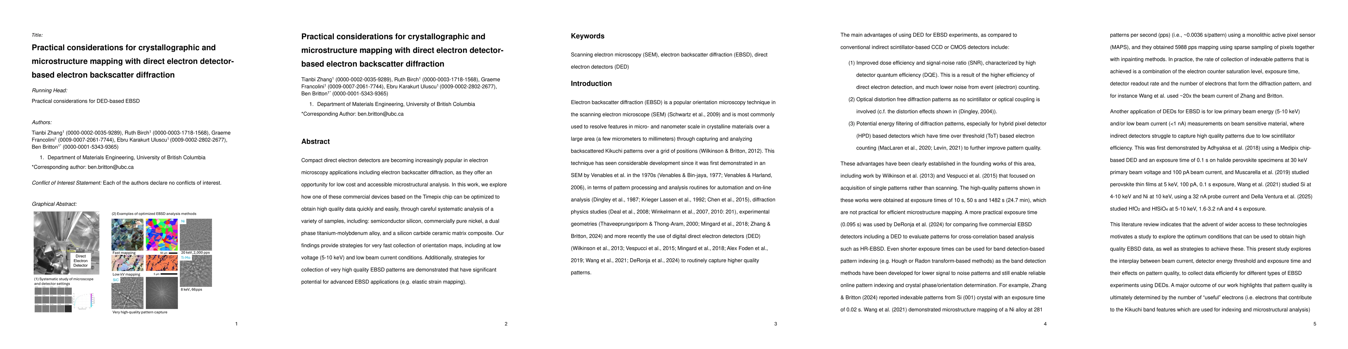
Compact direct electron detectors are becoming increasingly popular in electron microscopy applications including electron backscatter diffraction, as they offer an opportunity for low cost and accessible microstructural analysis. In this work, we explore how one of these commercial devices based on the Timepix chip can be optimized to obtain high quality data quickly and easily, through careful systematic analysis of a variety of samples, including: semiconductor silicon, commercially pure nickel, a dual phase titanium-molybdenum alloy, and a silicon carbide ceramic matrix composite. Our findings provide strategies for very fast collection of orientation maps, including at low voltage (5-10 keV) and low beam current conditions. Additionally, strategies for collection of very high quality EBSD patterns are demonstrated that have significant potential for advanced EBSD applications (e.g. elastic strain mapping).

AI Key Findings

Generated Jun 09, 2025

Methodology — What approach did the authors take?

The research methodology involved systematic analysis of various samples including semiconductor silicon, commercially pure nickel, a dual phase titanium-molybdenum alloy, and a silicon carbide ceramic matrix composite using a commercial device based on the Timepix chip for electron backscatter diffraction (EBSD) analysis.

Key Results — What are the main findings?

  • Strategies for fast collection of orientation maps at low voltage (5-10 keV) and low beam current conditions were demonstrated.
  • High-quality EBSD patterns were collected, showing potential for advanced EBSD applications such as elastic strain mapping.
  • Optimization of detector settings, primarily by adjusting primary beam energy, energy threshold, beam current, and exposure time, significantly improved pattern quality.

Significance — Why does this research matter?

This study highlights the effective use of a compact direct electron detector (DED) for routine EBSD analysis and its potential for advancing EBSD analysis by enabling high-quality and reliable EBSD data collection.

Technical Contribution — What is the technical contribution?

The paper presents a detailed method for tuning a DED for EBSD experiments, focusing on optimizing detector settings such as primary beam energy, energy threshold, beam current, and exposure time to achieve high-quality patterns.

Novelty — What is new about this work?

The work distinguishes itself by emphasizing the practical aspects of optimizing a commercial DED for EBSD, providing specific strategies for low-voltage and low-current conditions, and demonstrating its applicability for advanced EBSD applications.

Limitations — What are the limitations of this study?

  • The study was limited to specific materials and did not explore a wide range of sample types.
  • The performance of the Timepix-based DED might vary with other detector architectures or electron energies.

Future Work — What did the authors propose for future work?

  • Further exploration of DED optimization for diverse sample types and materials.
  • Investigating the compatibility and performance of the Timepix-based DED with other electron microscopy techniques.

Paper Details

Paper ID: 2504.11624
Comments: as submitted
Categories:
cond-mat.mtrl-sci

How to Cite This Paper

BibTeX
@article{britton2025practical,
  title         = {Practical considerations for crystallographic and microstructure mapping
  with direct electron detector-based electron backscatter diffraction},
  author        = {Britton, Ben and Uluscu, Ebru Karakurt and Francolini, Graeme and others},
  year          = {2025},
  eprint        = {2504.11624},
  archivePrefix = {arXiv},
  primaryClass  = {cond-mat.mtrl-sci},
}
APA 7
Britton, B., Uluscu, E., Francolini, G., Birch, R., & Zhang, T. (2025). Practical considerations for crystallographic and microstructure mapping
  with direct electron detector-based electron backscatter diffraction. arXiv. https://arxiv.org/abs/2504.11624
MLA 9
Britton, Ben, et al. "Practical considerations for crystallographic and microstructure mapping
  with direct electron detector-based electron backscatter diffraction." arXiv, 2025, arxiv.org/abs/2504.11624.

Citation Network

Current paper (gray), citations (green), references (blue)

Display is limited for performance on very large graphs.

Current Paper
Citations
References
Click to view

No citations found for this paper.

Comments (0)

This website uses cookies to ensure you get the best experience. Learn more